
 My Inquiry
 My Account


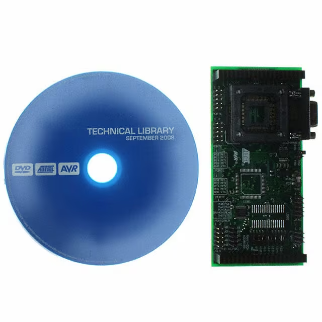
Microchip Technology ATSTK501
- Part No.:
- ATSTK501
- Manufacturer:
- Microchip Technology
- Category:
- Accessories
- Package:
- Datasheet:
-
 ATSTK501.pdf
- Description:
- ADAPTER KIT FOR 64PIN AVR MCU
- Quantity:
- Payment:

- Shipping:

Inventory:4,866
Please send an inquiry. Send us your inquiry, and we will respond immediately.
Product details
Overview
ATSTK501 from Microchip Technology (formerly Atmel) is a top-module evaluation board designed to extend the STK500 development system with full hardware support for ATmega103(L) and ATmega128(L) microcontrollers. It provides a ZIF socket for TQFP packages, JTAG debugging interface, dual-port RS-232C with RTS/CTS, external 128KB SRAM footprint, and dedicated PORT E/F/G/AUX I/O headers - enabling rapid prototyping of memory-intensive AVR applications including industrial control and embedded communications.
For engineers reviewing the ATSTK501 datasheet, ATSTK501 pinout, ATSTK501 application, or ATSTK501 equivalent, this page delivers verified technical context on SRAM address expansion (A16), software-controllable SRAMEN enable logic, TOSC switch configuration for 32 kHz RTC crystal routing, JTAG ICE compatibility, and jumper-based RAM high-address byte management - all critical for XRAM-enabled firmware development and hardware bring-up.
Technical Context
The ATSTK501 interfaces directly with the STK500 base board via EXPAND0/EXPAND1 headers and supports both in-system programming (ISP) and high-voltage parallel programming for ATmega103(L)/128(L). Its SRAM subsystem uses a 74AHC573 latch to drive A[7:0], with A16 routed separately and SRAMEN controlling chip-enable polarity (active-low).
Port expansion includes full PORT E (8-bit), PORT F (8-bit), and PORT G (5-bit + AUX signals: A16, SRAMEN, PEN), while the TOSC switch selectively routes PG3/PG4 between 32 kHz crystal or GPIO function. The RS-232C port implements logic-level translation via MAX3232ECAE and supports hardware flow control lines (RTS/CTS) for UART-based communication testing.
Key Specifications
| Parameter | Value and Actual Design Meaning |
|---|---|
| Form Factor | Top-module add-on board for STK500; requires STK500 base unit to operate. |
| Supported MCUs | ATmega103(L) and ATmega128(L); also enables SRAM interface for AT90S8515 and ATmega161 via manual signal strapping. |
| SRAM Interface | 128KB x8 footprint with A16, SRAMEN, and RAM high-address jumpers; supports software-controlled bank switching beyond 64KB limit. |
| Debug & Programming | JTAG connector compliant with Atmel JTAG ICE; ISP6PIN interface for SPI programming; HVPP support via PROGCTRL/PROGDATA routing. |
| Physical Dimensions | 56 mm × 119 mm × 27 mm; weight 70 g; 9-pin D-SUB female RS-232 connector. |
| Power Supply | 2.7V–5.5V operation; compatible with STK500's regulated VTG and AVTG rails. |
Availability
ATSTK501 is available at Aetrix Electronics and suitable for AVR microcontroller development, embedded firmware validation, and industrial control prototyping requiring stable component supply and legacy toolchain continuity.
Supply support for ATSTK501 includes scheduled delivery planning, volume procurement assistance, BOM continuity management, traceable sourcing, and lifecycle availability coordination for OEM customers, industrial embedded developers, connected-device designers, and electronics production programs.
Manufacturer
Microchip Technology acquired Atmel Corporation in 2016 and maintains full legacy support for AVR development tools. Atmel originally designed and qualified the STK501 for robustness in engineering labs and university teaching environments.
The ATSTK501 belongs to the STK500 ecosystem - a modular, expandable platform built to accelerate AVR MCU evaluation, debug, and production-ready firmware development across automotive, industrial, and consumer applications.
FAQ
What is the primary function of the ATSTK501 in the STK500 development system?
The ATSTK501 serves as a top-module expansion board that adds native hardware support for ATmega103(L) and ATmega128(L) microcontrollers to the STK500 base unit. It provides essential interfaces including ZIF socket for TQFP packages, JTAG debugging, external SRAM footprint, and extended I/O ports (PORT E/F/G), enabling full utilization of advanced features like XRAM and dual UARTs during firmware development and validation of ATSTK501-based designs.
Does the ATSTK501 require a separate power supply or is it powered by the STK500?
The ATSTK501 draws all operating power from the STK500 base board via the EXPAND0 and EXPAND1 headers - no external power supply is needed. It operates within the STK500's regulated VTG (target voltage) and AVTG (analog voltage) rails, supporting 2.7V–5.5V input range as specified in the ATSTK501 technical documentation.
How is external SRAM enabled and configured on the ATSTK501?
External SRAM is enabled on the ATSTK501 by connecting the SRAMEN pin (on PORTG/AUX header) to GND using a supplied jumper - asserting active-low chip-enable. The A16 signal controls upper memory bank selection, and RAM high-address jumpers configure Port C pins for address vs. general-purpose I/O. The ATSTK501 supports up to 128KB SRAM, with software-managed A16 toggling required to access beyond the default 64KB boundary.
Can the ATSTK501 be used with microcontrollers other than ATmega103(L) and ATmega128(L)?
Yes - the ATSTK501's SRAM interface and PORT headers can be adapted for AT90S8515 and ATmega161(L) using manual signal strapping (WR→PG0, RD→PG1, ALE→PG2) as documented in Section 2.8 of the ATSTK501 User Guide. However, JTAG debugging and PORT G functionality are exclusive to ATmega128(L), and ATmega103(L) lacks PORT G entirely - confirming ATSTK501's core compatibility remains focused on those two devices.
What is the role of the TOSC switch on the ATSTK501?
The TOSC switch on the ATSTK501 selects routing between the onboard 32 kHz crystal and PORT G pins PG3/TOSC2 and PG4/TOSC1. When engaged, the crystal connects directly to the ATmega128(L)'s oscillator inputs for real-time clock (RTC) applications; when disengaged, PG3 and PG4 become general-purpose I/O. This switch ensures flexible timing resource allocation without hardware modification - a key design feature confirmed in Section 2.9 of the ATSTK501 User Guide.
ATSTK501 Specifications
- Product attributes
- Attribute value
- Manufacturer:
- Microchip Technology
- Series:
- -
- Packaging:
- -
- Product Status:
- Obsolete
- Accessory Type:
- STK500 Expansion Module
- For Use With/Related Products:
- 64-pin megaAVR Devices
ATSTK501 FAQ
1.How can I place an order for ATSTK501 through Aetrix?
Please submit a Request for Quotation (RFQ) for ATSTK501 on Aetrix. Our sales agent will provide a competitive quotation and guide you through the order confirmation once you accept the terms.
2.Are the price and stock information for ATSTK501 reliable?
The price and inventory of ATSTK501 are updated periodically and may fluctuate due to market conditions. Stock and pricing data are typically refreshed every 24 hours. Quotation validity for ATSTK501 is usually 5 days.
3.What payment methods are accepted for ATSTK501?
We accept Wire Transfer, PayPal, Credit Card, Western Union, MoneyGram, and Escrow for ATSTK501 transactions.
Note: Certain payment methods may incur a processing fee.
4.How is shipping managed for ATSTK501?
ATSTK501 orders can be shipped via leading logistics carriers, including DHL, UPS, FedEx, TNT, or Registered Mail.
Once your ATSTK501 order is processed, you will receive an email with the shipment details and tracking number.
Note: Tracking information may take up to 24 hours to appear. Express delivery typically takes 3–5 business days.
5.How can I obtain technical support or documentation for ATSTK501?
For technical support, including ATSTK501 datasheets, pinout diagrams, or application guidance, please contact our engineering support team. They can provide detailed documentation and assistance for your ATSTK501 requirements.
6.How does Aetrix verify that ATSTK501 is sourced from the original manufacturer or authorized distributors?
All ATSTK501 products on Aetrix are procured from qualified distributors and authorized channels. Our dedicated quality assurance team conducts strict verification, including traceability checks and, if necessary, third-party testing. This ensures that ATSTK501 meets industry standards.
7.What is the process for return or replacement of ATSTK501?
All ATSTK501 units undergo pre-shipment inspection (PSI). If there is an issue with ATSTK501, returns or replacements are accepted under the following conditions:
1.Quantity discrepancies, incorrect items, or visible external defects (such as breakage or corrosion), acknowledged by Aetrix.
2.The issue is reported within 90 days of delivery.
3.The ATSTK501 part is unused and in its original packaging.
Return procedure for ATSTK501:
1.Submit a request within 90 days.
2.Obtain a Return Material Authorization (RMA) from Aetrix.
ATSTK501 Tags
-
261
Adafruit Industries LLC
-
5385
Adafruit Industries LLC
-
FIT0587
DFRobot
-
PRT-14427
SparkFun Electronics
-
PRT-10474
SparkFun Electronics
-
PRT-15109
SparkFun Electronics
-
PRT-11417
SparkFun Electronics
-
FIT0586
DFRobot

-
1131
Adafruit Industries LLC
-
MIKROE-485
MikroElektronika
-
2223
Adafruit Industries LLC
-
PRT-14017
SparkFun Electronics
Tech Hub

TTL and CMOS logic families differ in thresholds, loading, output drive, power and timing. This engineering guide compares 74HC and 74HCT, calculates noise margins and checks 3.3 V/5 V compatibility.

A practical engineering guide to 3.3V and 5V logic compatibility, input thresholds, resistor dividers, translator ICs, MOSFET level shifting, I2C pull-ups, timing limits and power-sequencing risks.

The 74HC595 uses push-pull logic outputs, while the TPIC6B595 uses 50 V open-drain DMOS sinks for higher-power loads. This guide compares timing, current limits, 3.3 V interfacing, load wiring, thermal…

The 74HC595 converts serial data into eight stable parallel outputs. This guide covers pin functions, shift and storage timing, OE and MR behavior, drive-current limits, cascading, voltage compatibilit…

A technical comparison of level-sensitive latches and edge-triggered flip-flops, covering timing windows, setup and hold limits, master–slave operation, time borrowing, race-through, HDL inference and…

A D latch stores one bit while Enable controls when data can pass. This reference covers gate-level operation, truth tables, transparency, setup and hold timing, LE versus OE, common ICs and practical …

An SR latch stores one bit through cross-coupled feedback. This engineering reference covers NOR and NAND implementations, truth tables, forbidden-state recovery, gated operation, switch debouncing, fa…

Latch circuits retain one bit through feedback. This technical reference covers SR and D latches, truth tables, transparency, timing limits, latch-versus-flip-flop behavior, applications and common log…

An engineering guide to LED driver operation, constant-current and constant-voltage outputs, linear and switching topologies, dimming, IC selection, calculations, replacement compatibility, and fault c…

Operational amplifier guide covering op amp basics, feedback, ideal vs real op amps, common configurations, buffer circuits, offset, bias current, gain-bandwidth, slew rate, rail-to-rail limits and sel…


