
 My Inquiry
 My Account


Microchip Technology ATWILC1000B-MU-T042
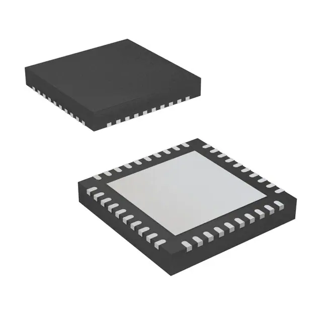
- Part No.:
- ATWILC1000B-MU-T042
- Manufacturer:
- Microchip Technology
- Category:
- RF Transceiver ICs
- Package:
- 40-VFQFN Exposed Pad
- Datasheet:
-
 ATWILC1000B-MU-T042.pdf
- Description:
- IC RF TXRX+MCU WIFI 40QFN
- Quantity:
- Payment:

- Shipping:

Inventory:6,688
Please send an inquiry. Send us your inquiry, and we will respond immediately.
Product details
Overview
ATWILC1000B-MU-T042 from Microchip Technology is an IEEE 802.11b/g/n single-stream (1×1) Wi-Fi SoC link controller with integrated PA, LNA, T/R switch, and power management. It delivers up to 72 Mbps PHY rate in the 2.4 GHz ISM band, operates from −40°C to +85°C, supports SPI/SDIO host interfaces, and achieves <1 μA deep power-down current at 3.3V I/O - optimized for battery-powered IoT edge nodes and portable medical sensors.
For engineers reviewing the ATWILC1000B-MU-T042 datasheet, ATWILC1000B-MU-T042 pinout, ATWILC1000B-MU-T042 application, or ATWILC1000B-MU-T042 equivalent, key selection criteria include its dual-host-interface flexibility (SPI/SDIO), on-chip memory management engine reducing host CPU load, hardware-accelerated A-MSDU/A-MPDU frame aggregation, WPA2-Enterprise security compliance, and QFN-40 package with exposed thermal paddle for RF grounding.
Technical Context
The ATWILC1000B-MU-T042 integrates a Cortus APS3 32-bit RISC processor handling MAC-layer functions including association, authentication, security key management, and beacon monitoring. Its WLAN subsystem implements OFDM PHY with advanced channel estimation, equalization, and carrier/timing synchronization - enabling robust operation in noisy 2.4 GHz environments.
It features dual clocking: a 26 MHz external crystal oscillator (±100 ppm initial offset, requiring calibration for ±25 ppm stability) and an internal 32 kHz ring oscillator (±10,000 ppm accuracy) used for low-power sleep timing. Power architecture includes dedicated supplies for RF TX/RX, digital core (VDDC), I/O (VDDIO), battery buck converter (VBATT_BUCK/VSW/VREG_BUCK), and tuner analog blocks (VDD_AMS/VDD_RF_TX/VDD_RF_RX).
Key Specifications
| Parameter | Value and Actual Design Meaning |
|---|---|
| Wi-Fi Standard | IEEE 802.11b/g/n, 20 MHz channel, 1×1 MIMO - enables cost-effective, low-complexity Wi-Fi connectivity without spatial multiplexing overhead. |
| PHY Data Rate | Up to 72 Mbps - maximum achievable physical layer throughput under ideal 20 MHz HT20 conditions with short GI. |
| Operating Temperature | −40°C to +85°C - qualified for industrial and automotive cabin-adjacent embedded applications. |
| I/O Supply Voltage | VDDIO = 1.62 V to 3.6 V - supports direct interfacing with 1.8 V or 3.3 V host microcontrollers without level shifters. |
| Battery Supply Range | VBATT = 3.0 V to 4.2 V - matches standard Li-ion/Li-poly battery discharge profiles for seamless integration. |
| Deep Power-Down Current | <1 μA at 3.3 V I/O - enables multi-year battery life in wake-on-event sensor nodes with infrequent transmissions. |
| Crystal Frequency | 26 MHz ±100 ppm - requires external 26 MHz crystal with ESR ≤150 Ω; internal 5 pF loading per pin must be compensated in PCB layout. |
Pinout & Package
The ATWILC1000B-MU-T042 is supplied in a 5 mm × 5 mm, 0.4 mm pitch, 40-pin QFN package with exposed thermal paddle (PADDLE VSS) that must be soldered to system ground for RF integrity and thermal dissipation.
| Pin/Terminal | Circuit Role | Design Meaning |
|---|---|---|
| SDIO_SPI_CFG | Interface Mode Select | Configures host interface: tied to GND for SDIO mode, pulled to VDDIO via 1 MΩ for SPI mode - determines pin function mapping for SD_DATx/SPI_SSN/SPI_TXD etc. |
| GPIO0/HOST_WAKEUP | Host Wake Control | Asserts active-low signal to wake host MCU from low-power state; firmware uses this pin for host-initiated wake events in Doze mode. |
| GPIO2/IRQN | Interrupt Output | Open-drain active-low interrupt output signaling packet arrival, connection status change, or error condition to host controller. |
| XO_P / XO_N | Differential Crystal Input | Accepts 26 MHz fundamental-mode crystal; internal 5 pF capacitance per pin requires precise external load capacitor calculation for frequency accuracy. |
| CHIP_EN | Global Device Enable | Active-high enable input; must be driven high by host after power stabilization to exit hardware reset and initialize internal regulators. |
| RESETN | Hard Reset Input | Active-low asynchronous reset; host must hold low ≥100 ns to force full device reinitialization, including register and RAM clearing. |
Key Features
| Feature | Design Value |
|---|---|
| Integrated RF Front-End | On-die PA, LNA, and T/R switch eliminate 6+ external RF components - reduces BOM count, PCB area, and matching complexity for 2.4 GHz band. |
| Hardware Frame Aggregation | Two-level A-MSDU/A-MPDU and Block Ack support - increases effective MAC throughput by up to 40% vs. legacy 802.11g in bursty traffic scenarios. |
| On-Chip Memory Management Engine | Offloads packet buffering, descriptor management, and DMA coordination from host CPU - reduces host firmware processing burden and memory footprint. |
| Wi-Fi Direct® & Soft-AP | Enables peer-to-peer connections and access point emulation without external AP hardware - supports standalone IoT gateway and local provisioning use cases. |
| Security Protocol Support | Firmware-implemented WEP, WPA, WPA2, and WPA2-Enterprise (802.1X/EAP-TLS) - meets enterprise-grade credential validation and encrypted session requirements. |
Applications
| Smart Home Sensor Node | Portable Medical Monitor |
|---|---|
Use Scenario: Battery-powered temperature/humidity sensor transmitting data every 5 minutes to cloud via home Wi-Fi router. IC Role / Device Role / Timing Role: Wi-Fi link controller managing association, secure TLS handshake, and low-duty-cycle beacon listening in Doze mode. Use Value: <1 μA deep power-down current extends CR2032 battery life beyond 3 years; integrated PA ensures reliable 20 m indoor range despite compact enclosure. | Use Scenario: Wearable ECG patch streaming real-time waveform to clinician tablet over local Wi-Fi network during ambulatory monitoring. IC Role / Device Role / Timing Role: Dual-role device acting as Soft-AP for direct tablet pairing and as STA for hospital network handoff - managed by firmware state machine. Use Value: Hardware-accelerated A-MPDU aggregation maintains >50 Mbps sustained throughput for lossless 12-lead waveform streaming; WPA2-Enterprise compliance satisfies HIPAA network policy. |
| Industrial Gateway Edge Module | Asset Tracking Tag |
Use Scenario: DIN-rail mounted gateway collecting Modbus RTU data from PLCs and forwarding via Wi-Fi to SCADA server. IC Role / Device Role / Timing Role: Host-controlled STA node performing periodic polling, TCP keep-alive, and firmware OTA updates over secured TLS channel. Use Value: SPI interface enables deterministic timing control from Cortex-M7 host; −40°C to +85°C rating ensures operation in unconditioned control cabinets. | Use Scenario: GPS-enabled logistics tag reporting location every 2 hours using Wi-Fi scanning in addition to cellular fallback. IC Role / Device Role / Timing Role: Low-power Wi-Fi scanner detecting nearby AP SSIDs and RSSI for coarse geo-fencing when GPS unavailable. Use Value: 380 μA Doze mode with preserved chip settings allows rapid beacon monitoring every 100 ms without full wake-up penalty - extends coin-cell lifetime to 5+ years. |
Equivalent & Alternatives
The following parts are listed as comparable options for similar Wi-Fi link controller applications.
| Alternative Part | Technical Difference | Application Difference | Selection Advice |
|---|---|---|---|
| ESP32-WROOM-32 | Integrated dual-core Xtensa LX6 MCU, 4 MB flash, Bluetooth LE - higher host compute capability but larger footprint and no WPA2-Enterprise firmware stack out-of-box. | Best suited for applications requiring embedded application logic, BLE coexistence, or OTA update autonomy - not drop-in replacement due to different SDK and security model. | Select when full MCU + Wi-Fi integration is needed and host offload is unnecessary; verify WPA2-Enterprise certification path with Espressif. |
| RTL8720DN | ARM Cortex-M23 core, 2 MB PSRAM, hardware crypto engine - superior AES/SHA acceleration but lacks integrated PA/LNA, requiring external RF front-end. | Preferred for high-throughput streaming with hardware crypto acceleration where RF design resources exist - adds 3–5 mm² PCB area and matching complexity. | Choose when cryptographic performance dominates RF integration trade-off; confirm antenna matching network compatibility with RTL8720DN reference design. |
Compared with ESP32-WROOM-32 and RTL8720DN, the ATWILC1000B-MU-T042 provides the smallest bill of materials for certified Wi-Fi connectivity with minimal host dependency, making it optimal for resource-constrained devices where RF integration, ultra-low sleep current, and enterprise security are non-negotiable.
Availability
ATWILC1000B-MU-T042 is available at Aetrix Electronics and suitable for smart home sensor nodes, portable medical monitors, industrial gateways, asset tracking tags, and Wi-Fi-enabled wearables requiring stable component supply across long-lifecycle production programs.
Supply support for ATWILC1000B-MU-T042 includes scheduled delivery planning, volume procurement assistance, BOM continuity management, traceable sourcing, and lifecycle availability coordination for OEM customers, industrial embedded developers, connected-device designers, and electronics production programs.
Manufacturer
Microchip Technology Inc. is a leading provider of microcontroller, analog, FPGA, and connectivity solutions, serving industrial, automotive, communications, and consumer markets with vertically integrated silicon and development tools.
The ATWILC1000B-MU-T042 belongs to Microchip's Wi-Fi SoC product line, designed specifically for ultra-low-power, certified 802.11b/g/n connectivity in space- and energy-constrained embedded systems - emphasizing RF integration, security compliance, and host interface flexibility.
FAQ
What host interfaces does the ATWILC1000B-MU-T042 support?
The ATWILC1000B-MU-T042 supports both SDIO and SPI host interfaces, selected via the SDIO_SPI_CFG pin. In SDIO mode, it uses SD_DAT0–3, SD_CMD, and SD_CLK signals; in SPI mode, the same pins map to SPI_TXD, SPI_RXD, SPI_SSN, and SPI_SCK. The ATWILC1000B-MU-T042 does not support UART or I²C for primary data transfer - those interfaces are reserved for debug and configuration only.
Does the ATWILC1000B-MU-T042 include a MAC address, and how is it stored?
Yes, the ATWILC1000B-MU-T042 variant with "042" suffix (as in ATWILC1000B-MU-T042) has a factory-programmed MAC address stored in Bank 0 of its 768-bit eFuse memory. This one-time-programmable memory also holds calibration data and firmware configuration bits. The ATWILC1000B-MU-T042 reads the MAC address during boot and exposes it via host driver APIs - no external EEPROM or software assignment is required.
What is the role of the CHIP_EN and RESETN pins on the ATWILC1000B-MU-T042?
CHIP_EN is an active-high enable pin that powers up internal regulators and releases the device from hardware power-down; it must be asserted after VDDIO and VBATT stabilize. RESETN is an active-low asynchronous reset pin that forces full register initialization and firmware reload. Both pins require proper host GPIO sequencing: CHIP_EN should be driven high before asserting RESETN high, and RESETN must remain low ≥100 ns. The ATWILC1000B-MU-T042 will not operate if either pin is left floating or incorrectly biased.
Can the ATWILC1000B-MU-T042 operate without an external 26 MHz crystal?
No - the ATWILC1000B-MU-T042 requires a 26 MHz fundamental-mode crystal connected to XO_P and XO_N pins for RF timing and baseband synchronization. While the device includes an internal 32 kHz ring oscillator for sleep timing, it lacks an internal RF clock source. The ATWILC1000B-MU-T042 datasheet specifies crystal ESR ≤150 Ω and recommends 5–12 pF external load capacitors depending on board parasitics and crystal tolerance.
What power-saving modes are available on the ATWILC1000B-MU-T042, and how do they differ?
The ATWILC1000B-MU-T042 offers three defined low-power states: Deep Power-Down (<1 μA, all circuits disabled except CHIP_EN detection), Doze mode (380 μA, registers retained, beacon monitoring active), and Sleep mode (on-chip 32 kHz oscillator running). In Doze mode, the ATWILC1000B-MU-T042 wakes rapidly via GPIO0 or SDIO transaction to process frames; Deep Power-Down requires full reinitialization. These modes are controlled exclusively by host firmware commands - no autonomous transitions occur.
ATWILC1000B-MU-T042 Specifications
- Product attributes
- Attribute value
- Manufacturer:
- Microchip Technology
- Series:
- -
- Package/Case:
- 40-VFQFN Exposed Pad
- Packaging:
- Tape & Reel (TR)
- Product Status:
- Active
- Programmable:
- Not Verified
- Type:
- TxRx + MCU
- RF Family/Standard:
- WiFi
- Protocol:
- 802.11b/g/n
- Modulation:
- CCK, DSSS, OFDM
- Frequency:
- 2.4GHz
- Data Rate (Max):
- 72.2Mbps
- Power - Output:
- 20.5dBm
- Sensitivity:
- -98dBm
- Memory Size:
- 128kB ROM, 224kB RAM
- Serial Interfaces:
- I2C, SDIO, SPI, UART
- GPIO:
- 9
- Voltage - Supply:
- 1.62V ~ 3.6V
- Current - Receiving:
- 52.5mA ~ 58.5mA
- Current - Transmitting:
- 244mA ~ 294mA
- Operating Temperature:
- -40°C ~ 85°C
- Grade:
- -
- Qualification:
- -
- Supplier Device Package:
- 40-QFN (5x5)
ATWILC1000B-MU-T042 FAQ
1.How can I place an order for ATWILC1000B-MU-T042 through Aetrix?
Please submit a Request for Quotation (RFQ) for ATWILC1000B-MU-T042 on Aetrix. Our sales agent will provide a competitive quotation and guide you through the order confirmation once you accept the terms.
2.Are the price and stock information for ATWILC1000B-MU-T042 reliable?
The price and inventory of ATWILC1000B-MU-T042 are updated periodically and may fluctuate due to market conditions. Stock and pricing data are typically refreshed every 24 hours. Quotation validity for ATWILC1000B-MU-T042 is usually 5 days.
3.What payment methods are accepted for ATWILC1000B-MU-T042?
We accept Wire Transfer, PayPal, Credit Card, Western Union, MoneyGram, and Escrow for ATWILC1000B-MU-T042 transactions.
Note: Certain payment methods may incur a processing fee.
4.How is shipping managed for ATWILC1000B-MU-T042?
ATWILC1000B-MU-T042 orders can be shipped via leading logistics carriers, including DHL, UPS, FedEx, TNT, or Registered Mail.
Once your ATWILC1000B-MU-T042 order is processed, you will receive an email with the shipment details and tracking number.
Note: Tracking information may take up to 24 hours to appear. Express delivery typically takes 3–5 business days.
5.How can I obtain technical support or documentation for ATWILC1000B-MU-T042?
For technical support, including ATWILC1000B-MU-T042 datasheets, pinout diagrams, or application guidance, please contact our engineering support team. They can provide detailed documentation and assistance for your ATWILC1000B-MU-T042 requirements.
6.How does Aetrix verify that ATWILC1000B-MU-T042 is sourced from the original manufacturer or authorized distributors?
All ATWILC1000B-MU-T042 products on Aetrix are procured from qualified distributors and authorized channels. Our dedicated quality assurance team conducts strict verification, including traceability checks and, if necessary, third-party testing. This ensures that ATWILC1000B-MU-T042 meets industry standards.
7.What is the process for return or replacement of ATWILC1000B-MU-T042?
All ATWILC1000B-MU-T042 units undergo pre-shipment inspection (PSI). If there is an issue with ATWILC1000B-MU-T042, returns or replacements are accepted under the following conditions:
1.Quantity discrepancies, incorrect items, or visible external defects (such as breakage or corrosion), acknowledged by Aetrix.
2.The issue is reported within 90 days of delivery.
3.The ATWILC1000B-MU-T042 part is unused and in its original packaging.
Return procedure for ATWILC1000B-MU-T042:
1.Submit a request within 90 days.
2.Obtain a Return Material Authorization (RMA) from Aetrix.
ATWILC1000B-MU-T042 Tags

-
ESP32-D0WD-V3
Espressif Systems

-
ESP8266EX
Espressif Systems

-
ESP32-S3
Espressif Systems

-
NRF24L01P-R7
Nordic Semiconductor ASA
-
NRF24L01P-R
Nordic Semiconductor ASA

-
ESP32-U4WDH
Espressif Systems

-
DA14531-00000OG2
Renesas
-
ESP32-C6FH4
Espressif Systems

-
DA14531-00000FX2
Renesas
-
NRF24L01P-T
Nordic Semiconductor ASA

-
NRF52810-QCAA-R
Nordic Semiconductor ASA
-
ESP32-S3FN8
Espressif Systems
Tech Hub

TTL and CMOS logic families differ in thresholds, loading, output drive, power and timing. This engineering guide compares 74HC and 74HCT, calculates noise margins and checks 3.3 V/5 V compatibility.

A practical engineering guide to 3.3V and 5V logic compatibility, input thresholds, resistor dividers, translator ICs, MOSFET level shifting, I2C pull-ups, timing limits and power-sequencing risks.

The 74HC595 uses push-pull logic outputs, while the TPIC6B595 uses 50 V open-drain DMOS sinks for higher-power loads. This guide compares timing, current limits, 3.3 V interfacing, load wiring, thermal…

The 74HC595 converts serial data into eight stable parallel outputs. This guide covers pin functions, shift and storage timing, OE and MR behavior, drive-current limits, cascading, voltage compatibilit…

A technical comparison of level-sensitive latches and edge-triggered flip-flops, covering timing windows, setup and hold limits, master–slave operation, time borrowing, race-through, HDL inference and…

A D latch stores one bit while Enable controls when data can pass. This reference covers gate-level operation, truth tables, transparency, setup and hold timing, LE versus OE, common ICs and practical …

An SR latch stores one bit through cross-coupled feedback. This engineering reference covers NOR and NAND implementations, truth tables, forbidden-state recovery, gated operation, switch debouncing, fa…

Latch circuits retain one bit through feedback. This technical reference covers SR and D latches, truth tables, transparency, timing limits, latch-versus-flip-flop behavior, applications and common log…

An engineering guide to LED driver operation, constant-current and constant-voltage outputs, linear and switching topologies, dimming, IC selection, calculations, replacement compatibility, and fault c…

Operational amplifier guide covering op amp basics, feedback, ideal vs real op amps, common configurations, buffer circuits, offset, bias current, gain-bandwidth, slew rate, rail-to-rail limits and sel…


