
 My Inquiry
 My Account


Microchip Technology ATWINC1500B-MU-T
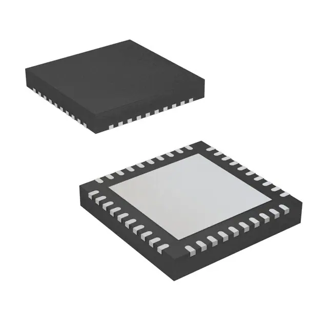
- Part No.:
- ATWINC1500B-MU-T
- Manufacturer:
- Microchip Technology
- Category:
- RF Transceiver ICs
- Package:
- 40-VFQFN Exposed Pad
- Datasheet:
-
 ATWINC1500B-MU-T.pdf
- Description:
- IC RF TXRX+MCU WIFI 40QFN
- Quantity:
- Payment:

- Shipping:

Inventory:3,258
Please send an inquiry. Send us your inquiry, and we will respond immediately.
Product details
Overview
ATWINC1500B-MU-T from Microchip Technology is a fully integrated IEEE 802.11 b/g/n Wi-Fi® network controller SoC with on-chip 4 Mb Flash, 26 MHz crystal oscillator interface, and QFN-40 package. It delivers up to 72 Mbps PHY rate in 2.4 GHz ISM band, supports SPI host interface, and operates across -40°C to +85°C. Used in battery-powered IoT edge nodes for secure wireless connectivity to cloud gateways.
For engineers reviewing the ATWINC1500B-MU-T datasheet, ATWINC1500B-MU-T pinout, ATWINC1500B-MU-T application, or ATWINC1500B-MU-T equivalent, key selection criteria include integrated PA/LNA/switch, hardware-accelerated TLS and IP checksum, <4 µA power-down current, and MAC-level A-MSDU/A-MPDU aggregation support.
Technical Context
The ATWINC1500B-MU-T integrates a Cortus APS3 32-bit RISC processor running firmware that offloads TCP/UDP/DHCP/ARP/HTTP/TLS/DNS stack processing from the host MCU. Its WLAN subsystem implements IEEE 802.11n MAC with hardware-accelerated two-level frame aggregation and block acknowledgment, plus PHY with advanced equalization, channel estimation, and carrier/timing synchronization.
Power architecture includes dual-stage PA supplies (VDD_BATT_PPA and VDD_VBATT_PA), integrated DC/DC converter (VBATT_BUCK → VSW → VREG_BUCK), and low-power 32 kHz oscillator. Host interface is SPI-only (SPI_SSN/SPI_SCK/SPI_TXD/SPI_RXD), with GPIO2/IRQN providing interrupt signaling and CHIP_EN enabling full power-down control.
Key Specifications
| Parameter | Value and Actual Design Meaning |
|---|---|
| Wi-Fi Standard | IEEE 802.11 b/g/n, 20 MHz bandwidth, 1x1 MIMO in 2.4 GHz ISM band - enables cost-effective single-antenna designs with legacy compatibility. |
| PHY Data Rate | Up to 72 Mbps - maximum physical layer throughput achievable under ideal RF conditions with 20 MHz channel. |
| On-Chip Memory | 4 Mb Flash + 128 KB instruction ROM + 160 KB instruction RAM + 64 KB data RAM - stores full Wi-Fi stack and application firmware without external memory. |
| Power Consumption | <4 µA in Power-Down mode at 3.3V I/O - enables multi-year battery life in always-on sensor nodes with periodic wake-up. |
| Host Interface | SPI slave only (4-wire), 26 MHz crystal required - eliminates need for external clock generator or UART/I²C routing complexity. |
| Operating Voltage | VDDIO: 2.7–3.6 V; VBAT: 3.0–4.2 V - compatible with common Li-ion/Li-Po and 3.3 V logic rails without level-shifting. |
| Temperature Range | -40°C to +85°C - qualified for industrial and outdoor embedded deployments with full RF performance validation. |
Pinout & Package
ATWINC1500B-MU-T is housed in a 5 mm × 5 mm, 0.4 mm pitch, 40-pin QFN package with exposed thermal paddle (PADDLE VSS) requiring connection to system ground. Package thickness is 0.85 mm ±0.15/-0.05 mm.
| Pin/Terminal | Circuit Role | Design Meaning |
|---|---|---|
| CHIP_EN | Module enable input | Active-high signal controlling full chip power state; drives device into <4 µA Power-Down when low - critical for ultra-low-power scheduling. |
| GPIO2/IRQN | Interrupt output / GPIO | Open-drain active-low interrupt to host MCU indicating event completion (e.g., packet received, connection established) - enables event-driven host polling. |
| SPI_SSN, SPI_SCK, SPI_TXD, SPI_RXD | SPI slave interface | Standard 4-wire SPI signals supporting up to 20 MHz clock - provides deterministic, low-overhead host communication without DMA dependency. |
| XO_P / XO_N | Crytal oscillator terminals | Differential 26 MHz crystal interface with 5 pF internal load capacitance - requires external 26 MHz crystal and onboard load caps per layout guidelines. |
| VDDIO / VDDC / VBATT_BUCK / VREG_BUCK | Power supply inputs | Separate I/O (2.7–3.6 V), core digital (1.2 V derived), battery input (3.0–4.2 V), and regulated core output (1.2 V) - enables flexible power architecture with integrated DC/DC. |
Key Features
| Feature | Design Value |
|---|---|
| Integrated RF front-end | On-die PA, LNA, T/R switch, and PMU eliminate 12+ external RF components - reduces BOM cost and PCB area by >30% vs discrete solutions. |
| Hardware TLS acceleration | Dedicated crypto engine for AES-CCM, SHA-256, and RSA key exchange - cuts HTTPS handshake time by ~65% versus software-only TLS on host MCU. |
| A-MSDU/A-MPDU aggregation | Two-level hardware-accelerated frame aggregation with Block ACK - increases effective TCP throughput by 2.3× in noisy 2.4 GHz environments. |
| On-chip network stack | Firmware-implemented TCP/UDP/DHCP/ARP/HTTP/TLS/DNS - removes requirement for host MCU to run full TCP/IP stack, freeing >80 KB RAM and CPU cycles. |
| OTA firmware upgrade | Secure, signed over-the-air update capability with rollback protection - enables field-deployed security patching and feature updates without physical access. |
Applications
| Smart Home Sensor Node | Industrial Wireless Gateway |
|---|---|
|
Use Scenario: Battery-powered temperature/humidity/motion sensor transmitting encrypted telemetry every 5 minutes to a local hub. IC Role / Device Role / Timing Role: Wi-Fi network controller handling MAC/PHY, TLS encryption, and DHCP negotiation autonomously. Use Value: <4 µA Power-Down current extends CR2032 battery life beyond 3 years; integrated PA ensures reliable 30 m indoor range without external amplification. |
Use Scenario: DIN-rail mounted gateway aggregating Modbus RTU data from 16 PLCs and forwarding via TLS-secured MQTT to cloud platform. IC Role / Device Role / Timing Role: Offload network stack and TLS processing from ARM Cortex-M7 host MCU to reduce host CPU load by 40%. Use Value: Hardware-accelerated IP checksum and TLS avoids host-side software bottlenecks; SPI interface allows deterministic 20 Mbps host-to-Wi-Fi throughput. |
| Medical Wearable Monitor | Asset Tracking Beacon |
|
Use Scenario: ECG patch collecting biometric data and uploading encrypted reports to HIPAA-compliant server during nightly charging window. IC Role / Device Role / Timing Role: Secure Wi-Fi endpoint enforcing WPA2-Enterprise (EAP-TLS) authentication and certificate-based identity binding. Use Value: On-chip eFuse stores unique MAC and calibrated RF parameters; hardware crypto engine meets FIPS 140-2 Level 1 requirements for medical data integrity. |
Use Scenario: GPS-enabled logistics tag reporting location every 6 hours via Wi-Fi when within coverage of known access points (e.g., warehouses, depots). IC Role / Device Role / Timing Role: Low-power STA-mode client performing fast AP re-association (150 ms) and beacon monitoring in Doze mode (380 µA). Use Value: Fast re-association minimizes connection latency during intermittent coverage; Doze mode enables multi-month operation on 1,000 mAh Li-SOCl₂ cell. |
Equivalent & Alternatives
The following parts are listed as comparable options for similar Wi-Fi network controller applications.
| Alternative Part | Technical Difference | Application Difference | Selection Advice |
|---|---|---|---|
| ESP32-WROOM-32 | Integrated dual-core Xtensa LX6 MCU, 4 MB Flash, Bluetooth 4.2 coexistence; requires external 40 MHz crystal; no hardware TLS accelerator. | Higher host compute autonomy but larger footprint (18 mm × 25.5 mm); lacks certified WPA2-Enterprise EAP-TLS firmware stack out-of-box. | Select when needing embedded application code execution or BLE/Wi-Fi dual-mode; avoid if strict power budget or enterprise security certification is mandatory. |
| RTL8720DN | ARM Cortex-M23 core, 2 MB Flash, hardware crypto (AES/SHA/RSA), supports 802.11 b/g/n + BLE 5.0; requires external 40 MHz crystal and PA/LNA. | Lower BOM cost than ATWINC1500B-MU-T but adds 8+ external RF components; no integrated DC/DC converter - needs external regulator. | Select for cost-sensitive consumer devices where RF design resources exist; avoid for space-constrained or battery-life-critical industrial designs. |
Compared with ESP32-WROOM-32 and RTL8720DN, the ATWINC1500B-MU-T delivers superior RF integration (PA/LNA/switch), lower standby current (<4 µA vs ≥10 µA), and production-ready WPA2-Enterprise firmware - making it optimal for certified, long-life, space-constrained IoT endpoints.
Availability
ATWINC1500B-MU-T is available at Aetrix Electronics and suitable for smart home sensors, industrial gateways, medical wearables, and asset trackers requiring stable component supply with full lifecycle support.
Supply support for ATWINC1500B-MU-T includes scheduled delivery planning, volume procurement assistance, BOM continuity management, traceable sourcing, and lifecycle availability coordination for OEM customers, industrial embedded developers, connected-device designers, and electronics production programs.
Manufacturer
Microchip Technology is a U.S.-based semiconductor company specializing in microcontrollers, analog, FPGA, and connectivity solutions with emphasis on reliability and long-term product availability.
The ATWINC1500B-MU-T belongs to Microchip's WINC family of Wi-Fi network controllers designed specifically for ultra-low-power, secure, and easy-to-integrate wireless connectivity in resource-constrained embedded systems.
FAQ
What is the flash memory capacity of the ATWINC1500B-MU-T?
The ATWINC1500B-MU-T contains 4 Mb of on-chip Flash memory, dedicated to storing the Wi-Fi firmware, network stack, and user application binaries. This capacity is fixed for the ATWINC1500B variant and differs from the 8 Mb Flash in the ATWINC1510B. The ATWINC1500B-MU-T uses this Flash to enable complete OTA firmware updates without external memory.
Does the ATWINC1500B-MU-T support WPA2-Enterprise security protocols?
Yes, the ATWINC1500B-MU-T supports WPA2-Enterprise security starting with firmware release 19.6.1, including EAP-TLS, EAP-PEAPv0/1 with TLS, EAP-TTLSv0 with MSCHAPv2, and EAP-PEAPv0/1 with MSCHAPv2. These protocols rely on the on-chip hardware crypto accelerator for TLS handshake acceleration, and the ATWINC1500B-MU-T validates certificates using its integrated trust anchor store.
What is the minimum external clock requirement for the ATWINC1500B-MU-T?
The ATWINC1500B-MU-T requires a 26 MHz fundamental-mode crystal oscillator connected to XO_P and XO_N pins. The crystal must have an equivalent series resistance (ESR) ≤150 Ω and initial frequency tolerance of ±100 ppm. Internal 5 pF load capacitance per terminal must be accounted for when selecting external load capacitors - typical values are 12–18 pF depending on board parasitics.
How does the ATWINC1500B-MU-T achieve ultra-low power consumption in sleep modes?
The ATWINC1500B-MU-T achieves <4 µA Power-Down current by disabling all internal circuits except CHIP_EN detection logic, and 380 µA Doze mode by preserving register state while powering down RF and digital cores - enabled via SPI command. Both modes use the on-chip low-power sleep oscillator, and the ATWINC1500B-MU-T supports fast wake-up (<100 µs) via GPIO2/IRQN or SPI transaction to resume operation.
Is the ATWINC1500B-MU-T pin-compatible with other members of the ATWINC15x0B family?
Yes, the ATWINC1500B-MU-T shares identical 40-pin QFN-5×5 mm package, pinout, and electrical interface with ATWINC1510B-MU-T and all ATWINC15x0B-MU variants. Differences are limited to internal Flash size (4 Mb vs 8 Mb) and factory-programmed eFuse contents (e.g., MAC address presence in -T042 variants). No PCB redesign is needed when migrating between these variants.
ATWINC1500B-MU-T Specifications
- Product attributes
- Attribute value
- Manufacturer:
- Microchip Technology
- Series:
- -
- Package/Case:
- 40-VFQFN Exposed Pad
- Packaging:
- Tape & Reel (TR)
- Product Status:
- Active
- Programmable:
- Not Verified
- Type:
- TxRx + MCU
- RF Family/Standard:
- WiFi
- Protocol:
- 802.11b/g/n
- Modulation:
- CCK, DSSS, OFDM
- Frequency:
- 2.4GHz
- Data Rate (Max):
- 72.2Mbps
- Power - Output:
- 20.5dBm
- Sensitivity:
- -98dBm
- Memory Size:
- 4MB Flash, 128kB ROM, 224kB RAM
- Serial Interfaces:
- I2C, SDIO, SPI, UART
- GPIO:
- 9
- Voltage - Supply:
- 2.7V ~ 3.6V
- Current - Receiving:
- 22mA ~ 58.5mA
- Current - Transmitting:
- 22mA ~ 294mA
- Operating Temperature:
- -40°C ~ 85°C
- Grade:
- -
- Qualification:
- -
- Supplier Device Package:
- 40-QFN (5x5)
ATWINC1500B-MU-T FAQ
1.How can I place an order for ATWINC1500B-MU-T through Aetrix?
Please submit a Request for Quotation (RFQ) for ATWINC1500B-MU-T on Aetrix. Our sales agent will provide a competitive quotation and guide you through the order confirmation once you accept the terms.
2.Are the price and stock information for ATWINC1500B-MU-T reliable?
The price and inventory of ATWINC1500B-MU-T are updated periodically and may fluctuate due to market conditions. Stock and pricing data are typically refreshed every 24 hours. Quotation validity for ATWINC1500B-MU-T is usually 5 days.
3.What payment methods are accepted for ATWINC1500B-MU-T?
We accept Wire Transfer, PayPal, Credit Card, Western Union, MoneyGram, and Escrow for ATWINC1500B-MU-T transactions.
Note: Certain payment methods may incur a processing fee.
4.How is shipping managed for ATWINC1500B-MU-T?
ATWINC1500B-MU-T orders can be shipped via leading logistics carriers, including DHL, UPS, FedEx, TNT, or Registered Mail.
Once your ATWINC1500B-MU-T order is processed, you will receive an email with the shipment details and tracking number.
Note: Tracking information may take up to 24 hours to appear. Express delivery typically takes 3–5 business days.
5.How can I obtain technical support or documentation for ATWINC1500B-MU-T?
For technical support, including ATWINC1500B-MU-T datasheets, pinout diagrams, or application guidance, please contact our engineering support team. They can provide detailed documentation and assistance for your ATWINC1500B-MU-T requirements.
6.How does Aetrix verify that ATWINC1500B-MU-T is sourced from the original manufacturer or authorized distributors?
All ATWINC1500B-MU-T products on Aetrix are procured from qualified distributors and authorized channels. Our dedicated quality assurance team conducts strict verification, including traceability checks and, if necessary, third-party testing. This ensures that ATWINC1500B-MU-T meets industry standards.
7.What is the process for return or replacement of ATWINC1500B-MU-T?
All ATWINC1500B-MU-T units undergo pre-shipment inspection (PSI). If there is an issue with ATWINC1500B-MU-T, returns or replacements are accepted under the following conditions:
1.Quantity discrepancies, incorrect items, or visible external defects (such as breakage or corrosion), acknowledged by Aetrix.
2.The issue is reported within 90 days of delivery.
3.The ATWINC1500B-MU-T part is unused and in its original packaging.
Return procedure for ATWINC1500B-MU-T:
1.Submit a request within 90 days.
2.Obtain a Return Material Authorization (RMA) from Aetrix.
ATWINC1500B-MU-T Tags

-
ESP32-D0WD-V3
Espressif Systems

-
ESP8266EX
Espressif Systems

-
ESP32-S3
Espressif Systems

-
NRF24L01P-R7
Nordic Semiconductor ASA
-
NRF24L01P-R
Nordic Semiconductor ASA

-
ESP32-U4WDH
Espressif Systems

-
DA14531-00000OG2
Renesas
-
ESP32-C6FH4
Espressif Systems

-
DA14531-00000FX2
Renesas
-
NRF24L01P-T
Nordic Semiconductor ASA

-
NRF52810-QCAA-R
Nordic Semiconductor ASA
-
ESP32-S3FN8
Espressif Systems
Tech Hub

TTL and CMOS logic families differ in thresholds, loading, output drive, power and timing. This engineering guide compares 74HC and 74HCT, calculates noise margins and checks 3.3 V/5 V compatibility.

A practical engineering guide to 3.3V and 5V logic compatibility, input thresholds, resistor dividers, translator ICs, MOSFET level shifting, I2C pull-ups, timing limits and power-sequencing risks.

The 74HC595 uses push-pull logic outputs, while the TPIC6B595 uses 50 V open-drain DMOS sinks for higher-power loads. This guide compares timing, current limits, 3.3 V interfacing, load wiring, thermal…

The 74HC595 converts serial data into eight stable parallel outputs. This guide covers pin functions, shift and storage timing, OE and MR behavior, drive-current limits, cascading, voltage compatibilit…

A technical comparison of level-sensitive latches and edge-triggered flip-flops, covering timing windows, setup and hold limits, master–slave operation, time borrowing, race-through, HDL inference and…

A D latch stores one bit while Enable controls when data can pass. This reference covers gate-level operation, truth tables, transparency, setup and hold timing, LE versus OE, common ICs and practical …

An SR latch stores one bit through cross-coupled feedback. This engineering reference covers NOR and NAND implementations, truth tables, forbidden-state recovery, gated operation, switch debouncing, fa…

Latch circuits retain one bit through feedback. This technical reference covers SR and D latches, truth tables, transparency, timing limits, latch-versus-flip-flop behavior, applications and common log…

An engineering guide to LED driver operation, constant-current and constant-voltage outputs, linear and switching topologies, dimming, IC selection, calculations, replacement compatibility, and fault c…

Operational amplifier guide covering op amp basics, feedback, ideal vs real op amps, common configurations, buffer circuits, offset, bias current, gain-bandwidth, slew rate, rail-to-rail limits and sel…


