
 My Inquiry
 My Account


Microchip Technology ATWINC1500B-MU-Y042
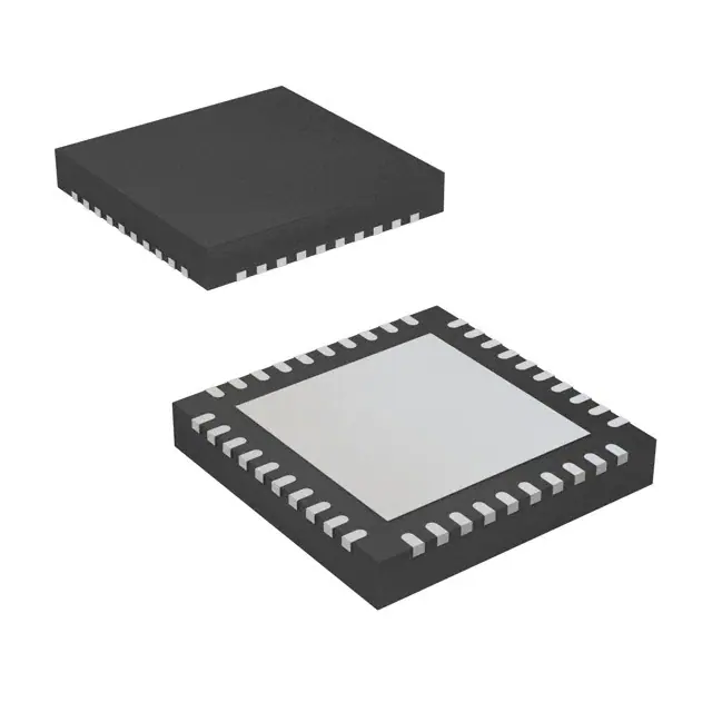
- Part No.:
- ATWINC1500B-MU-Y042
- Manufacturer:
- Microchip Technology
- Category:
- RF Transceiver ICs
- Package:
- 40-VFQFN Exposed Pad
- Datasheet:
-
 ATWINC1500B-MU-Y042.pdf
- Description:
- IC RF TXRX+MCU WIFI 40QFN
- Quantity:
- Payment:

- Shipping:

Inventory:953
Please send an inquiry. Send us your inquiry, and we will respond immediately.
Product details
Overview
ATWINC1500B-MU-Y042 from Microchip Technology is a fully integrated IEEE 802.11b/g/n Wi-Fi SoC with on-chip 32-bit Cortus APS3 processor, 4 Mb Flash, and hardware-accelerated TCP/IP stack. It delivers up to 72 Mbps PHY rate in 2.4 GHz ISM band, supports Soft-AP mode, WPA2 security, and operates from -40°C to +85°C with I/O voltage 2.7–3.6 V. It interfaces via SPI to host MCUs in battery-powered IoT sensor nodes.
For engineers reviewing the ATWINC1500B-MU-Y042 datasheet, ATWINC1500B-MU-Y042 pinout, ATWINC1500B-MU-Y042 application, or ATWINC1500B-MU-Y042 equivalent, key selection considerations include its 40-pin QFN (5×5 mm) package, MAC ID pre-programmed, <4 µA power-down current, integrated PA/LNA/switch, and SPI-only host interface without UART/I²C functional use in production firmware.
Technical Context
The ATWINC1500B-MU-Y042 implements a dedicated WLAN MAC with hardware-accelerated A-MSDU/A-MPDU aggregation and block acknowledgment, alongside a programmable Cortus APS3 core handling association, security key management, and TLS offload. Its PHY employs advanced equalization, channel estimation, and carrier/timing synchronization for robust 20 MHz 1×1 MIMO operation.
Power architecture integrates a DC/DC buck converter (VBAT 3.0–4.2 V input), low-power 32 kHz ring oscillator, and five distinct sleep modes-including Doze mode (380 µA) with beacon monitoring and <4 µA Power Down-enabled via CHIP_EN and RESETN control pins. All RF and analog supplies (VDD_RF_TX, VDD_AMS, VDD_SXDIG, etc.) are separately decoupled per datasheet layout guidelines.
Key Specifications
| Parameter | Value and Actual Design Meaning |
|---|---|
| Wi-Fi Standard | IEEE 802.11b/g/n, 2.4 GHz ISM band only, 20 MHz channel bandwidth |
| PHY Data Rate | Up to 72 Mbps (1×1 SISO, MCS7 @ 20 MHz) |
| Memory | 4 Mb on-chip Flash (pre-programmed with MAC ID), 128 KB ROM, 160 KB IRAM, 64 KB DRAM |
| Host Interface | SPI slave only (MOSI/MISO/SCK/SSN); UART and I²C pins present but debug-only, not enabled in production firmware |
| Power Consumption | <4 µA in Power Down mode (3.3 V I/O), 380 µA in Doze mode with beacon monitoring |
| Operating Voltage | VDDIO = 2.7–3.6 V; VBAT = 3.0–4.2 V (DC/DC input); crystal = 26 MHz ±100 ppm |
| Temperature Range | -40°C to +85°C ambient; RF performance characterized at 25°C with ≤3 dB variation at extremes |
Pinout & Package
The ATWINC1500B-MU-Y042 is housed in a 40-pin QFN package (5 mm × 5 mm, 0.4 mm pitch) with exposed thermal paddle requiring PCB ground connection. Pin functions are validated per Microchip DS70005374B, pages 6–9.
| Pin/Terminal | Circuit Role | Design Meaning |
|---|---|---|
| SPI_SSN | Digital I/O (active-low) | Slave select signal; must be driven by host MCU to initiate SPI transactions |
| SPI_SCK | Digital I/O | Clock input synchronized to host; determines maximum SPI speed (up to 20 MHz) |
| SPI_TXD | Digital I/O (MISO) | Serial data output from ATWINC1500B-MU-Y042 to host MCU |
| SPI_RXD | Digital I/O (MOSI) | Serial data input from host MCU to ATWINC1500B-MU-Y042 |
| GPIO2/IRQN | Digital I/O / Interrupt output | Open-drain interrupt signal indicating event completion (e.g., packet received, connection state change) |
| CHIP_EN | Analog input | Active-high enable; drives module into Power Down mode when low; requires 1 MΩ pull-down at power-up if host GPIO is tristated |
| RESETN | Digital input (active-low) | Hard reset control; must be held low ≥100 ns then released to enter Normal state |
| XO_P / XO_N | Analog differential | 26 MHz crystal connections; internal 5 pF load per pin; external loading capacitance must account for on-board Conboard |
| VDDIO | Power supply | Digital I/O rail (2.7–3.6 V); powers SPI/UART/GPIO logic; separate from core (VDDC) and RF supplies |
| PADDLE VSS | Power ground | Exposed thermal pad; must be soldered to solid PCB ground plane for thermal and EMI performance |
Key Features
| Feature | Design Value |
|---|---|
| Hardware-accelerated network stack | On-chip TCP/UDP/DHCP/ARP/HTTP/TLS/DNS reduces host MCU RAM/CPU load; no external protocol stack required |
| Integrated RF front-end | Fully embedded PA, LNA, T/R switch, and PMU eliminate discrete RF components and reduce BOM count |
| Security acceleration | Dedicated cipher engine handles WEP/WPA-TKIP/WPA2-CCMP-AES encryption/decryption and TLS handshake offload |
| OTA firmware upgrade | Complete system firmware update over Wi-Fi without host intervention or physical access |
| Low-power sleep architecture | Chip-level power gating and dedicated 32 kHz oscillator enable sub-millisecond wake-up from Doze mode for beacon listening |
Applications
| Smart Home Sensor Node | Industrial Wireless Gateway |
|---|---|
Use Scenario: Battery-powered temperature/humidity sensor transmitting data hourly to cloud via home Wi-Fi router. IC Role / Device Role / Timing Role: Standalone Wi-Fi SoC managing link establishment, TLS-secured MQTT transmission, and deep-sleep scheduling. Use Value: <4 µA Power Down current extends 2-AA battery life beyond 5 years; integrated Flash stores credentials and firmware patches. | Use Scenario: DIN-rail mounted gateway collecting Modbus RTU data from PLCs and bridging to enterprise Wi-Fi infrastructure. IC Role / Device Role / Timing Role: Host-independent network controller providing secure AP mode for local device onboarding and STA mode for upstream cloud connectivity. Use Value: Hardware-accelerated TLS and dual-mode (STA+Soft-AP) operation enable simultaneous secure local commissioning and remote telemetry without host CPU overhead. |
| Medical Wearable Monitor | Asset Tracking Tag |
Use Scenario: Chest-worn ECG patch uploading encrypted waveform snippets to HIPAA-compliant server during brief Wi-Fi connection windows. IC Role / Device Role / Timing Role: Low-latency Wi-Fi transceiver with fast AP re-association (150 ms) and hardware IP checksum offload. Use Value: 380 µA Doze mode preserves battery between transmissions; on-chip memory management engine minimizes host DMA buffer management burden. | Use Scenario: GPS-enabled logistics tag reporting location every 6 hours via public Wi-Fi hotspots in warehouses and transport hubs. IC Role / Device Role / Timing Role: Autonomous network joiner using pre-stored SSID/PSK, performing passive scan, and initiating TLS handshakes without host coordination. Use Value: Pre-programmed MAC ID (Y042 suffix) ensures unique identity; integrated eFuse stores calibrated TX power and crystal offset for consistent RF performance across units. |
Equivalent & Alternatives
The following parts are listed as comparable options for similar Wi-Fi SoC applications.
| Alternative Part | Technical Difference | Application Difference | Selection Advice |
|---|---|---|---|
| ATWINC1510B-MU-Y042 | 8 Mb Flash (vs. 4 Mb), same pinout, identical RF/performance specs, firmware-compatible | Required when larger OTA firmware images, extended certificate storage, or future feature expansion needed | Select ATWINC1510B-MU-Y042 only if >4 Mb Flash capacity is confirmed necessary; otherwise ATWINC1500B-MU-Y042 offers cost and footprint advantage |
| ESP32-WROOM-32 | Integrated dual-core Xtensa LX6 MCU, Bluetooth LE, 4 MB PSRAM option, 3.3 V only, no DC/DC converter | Suitable for host-less applications needing rich local processing; less optimal for ultra-low-power intermittent transmit duty cycles | Choose ESP32-WROOM-32 when Bluetooth coexistence, local AI inference, or high-speed USB/JTAG debug is required; ATWINC1500B-MU-Y042 remains superior for minimal-power, SPI-hosted designs |
Compared with ATWINC1510B-MU-Y042, ATWINC1500B-MU-Y042 provides identical RF performance and power efficiency at lower Flash cost and smaller firmware memory footprint; versus ESP32-WROOM-32, it delivers deeper sleep currents and simpler SPI integration but lacks embedded application processing and Bluetooth.
Availability
ATWINC1500B-MU-Y042 is available at Aetrix Electronics and suitable for smart home sensors, medical wearables, industrial gateways, and asset tracking tags requiring stable component supply, pre-programmed MAC identity, and long-term lifecycle support.
Supply support for ATWINC1500B-MU-Y042 includes scheduled delivery planning, volume procurement assistance, BOM continuity management, traceable sourcing, and lifecycle availability coordination for OEM customers, industrial embedded developers, connected-device designers, and electronics production programs.
Manufacturer
Microchip Technology Inc. is a U.S.-based semiconductor company specializing in microcontrollers, analog devices, and connectivity solutions for embedded systems.
The ATWINC15x0B product line was designed specifically for ultra-low-power, host-processor-offloaded Wi-Fi applications in battery-constrained IoT endpoints, emphasizing minimal external components and certified interoperability.
FAQ
What is the primary function of the ATWINC1500B-MU-Y042 in an embedded system?
The ATWINC1500B-MU-Y042 serves as a standalone Wi-Fi network controller SoC that handles all IEEE 802.11b/g/n MAC/PHY operations, TCP/IP stack processing, and TLS security acceleration. It relieves the host MCU of Wi-Fi protocol complexity, enabling simple SPI-based communication while maintaining ultra-low power consumption. The ATWINC1500B-MU-Y042 integrates Flash, RAM, and RF front-end to minimize external components.
Does the ATWINC1500B-MU-Y042 support UART or I²C for host communication?
No - although UART_TXD, UART_RXD, I2C_SDA, and I2C_SCL pins are physically present on the ATWINC1500B-MU-Y042 package, they are designated for debug and testing only per Microchip's official documentation. Production firmware does not enable these interfaces; the sole supported host interface is SPI (SPI_SSN, SPI_SCK, SPI_TXD, SPI_RXD). Using UART or I²C in final design violates specification and risks undefined behavior.
What does the "Y042" suffix indicate in ATWINC1500B-MU-Y042?
The "Y042" suffix indicates two specific factory-configured attributes: "Y" denotes tray packaging, and "042" signifies that the unit has a unique, pre-programmed MAC address stored in eFuse Bank 1. This eliminates post-manufacturing MAC provisioning steps and ensures IEEE-compliant uniqueness out-of-box. The ATWINC1500B-MU-Y042 also contains 4 Mb Flash, distinguishing it from the 8 Mb ATWINC1510B variant.
How does the ATWINC1500B-MU-Y042 achieve ultra-low power consumption in battery-operated devices?
The ATWINC1500B-MU-Y042 achieves ultra-low power through multiple hardware-enforced states: <4 µA Power Down mode (all circuits gated except CHIP_EN detection), 380 µA Doze mode (retains register context and monitors beacons), and fast wake-up (<1 ms) via IRQN or SPI activity. Its integrated DC/DC converter optimizes battery-to-core voltage conversion, and the on-chip 32 kHz oscillator enables precise timing without external crystals in sleep states. These features make ATWINC1500B-MU-Y042 ideal for multi-year battery life in intermittent transmit applications.
Is the ATWINC1500B-MU-Y042 pin-compatible with other members of the ATWINC15x0B family?
Yes - the ATWINC1500B-MU-Y042 shares identical 40-pin QFN (5×5 mm) mechanical and electrical pinout with ATWINC1510B-MU-Y042 and all ATWINC15x0B variants. Signal mapping, power domains, and timing specifications are fully aligned. Firmware and hardware design can be reused across the family; the primary differentiation lies in Flash size (4 Mb vs. 8 Mb) and eFuse programming (MAC ID presence), not pin functionality or layout.
ATWINC1500B-MU-Y042 Specifications
- Product attributes
- Attribute value
- Manufacturer:
- Microchip Technology
- Series:
- -
- Package/Case:
- 40-VFQFN Exposed Pad
- Packaging:
- Tray
- Product Status:
- Active
- Programmable:
- Not Verified
- Type:
- TxRx + MCU
- RF Family/Standard:
- WiFi
- Protocol:
- 802.11b/g/n
- Modulation:
- CCK, DSSS, OFDM
- Frequency:
- 2.4GHz
- Data Rate (Max):
- 72.2Mbps
- Power - Output:
- 20.5dBm
- Sensitivity:
- -98dBm
- Memory Size:
- 4MB Flash, 128kB ROM, 224kB RAM
- Serial Interfaces:
- I2C, SDIO, SPI, UART
- GPIO:
- 9
- Voltage - Supply:
- 2.7V ~ 3.6V
- Current - Receiving:
- 22mA ~ 58.5mA
- Current - Transmitting:
- 22mA ~ 294mA
- Operating Temperature:
- -40°C ~ 85°C
- Grade:
- -
- Qualification:
- -
- Supplier Device Package:
- 40-QFN (5x5)
ATWINC1500B-MU-Y042 FAQ
1.How can I place an order for ATWINC1500B-MU-Y042 through Aetrix?
Please submit a Request for Quotation (RFQ) for ATWINC1500B-MU-Y042 on Aetrix. Our sales agent will provide a competitive quotation and guide you through the order confirmation once you accept the terms.
2.Are the price and stock information for ATWINC1500B-MU-Y042 reliable?
The price and inventory of ATWINC1500B-MU-Y042 are updated periodically and may fluctuate due to market conditions. Stock and pricing data are typically refreshed every 24 hours. Quotation validity for ATWINC1500B-MU-Y042 is usually 5 days.
3.What payment methods are accepted for ATWINC1500B-MU-Y042?
We accept Wire Transfer, PayPal, Credit Card, Western Union, MoneyGram, and Escrow for ATWINC1500B-MU-Y042 transactions.
Note: Certain payment methods may incur a processing fee.
4.How is shipping managed for ATWINC1500B-MU-Y042?
ATWINC1500B-MU-Y042 orders can be shipped via leading logistics carriers, including DHL, UPS, FedEx, TNT, or Registered Mail.
Once your ATWINC1500B-MU-Y042 order is processed, you will receive an email with the shipment details and tracking number.
Note: Tracking information may take up to 24 hours to appear. Express delivery typically takes 3–5 business days.
5.How can I obtain technical support or documentation for ATWINC1500B-MU-Y042?
For technical support, including ATWINC1500B-MU-Y042 datasheets, pinout diagrams, or application guidance, please contact our engineering support team. They can provide detailed documentation and assistance for your ATWINC1500B-MU-Y042 requirements.
6.How does Aetrix verify that ATWINC1500B-MU-Y042 is sourced from the original manufacturer or authorized distributors?
All ATWINC1500B-MU-Y042 products on Aetrix are procured from qualified distributors and authorized channels. Our dedicated quality assurance team conducts strict verification, including traceability checks and, if necessary, third-party testing. This ensures that ATWINC1500B-MU-Y042 meets industry standards.
7.What is the process for return or replacement of ATWINC1500B-MU-Y042?
All ATWINC1500B-MU-Y042 units undergo pre-shipment inspection (PSI). If there is an issue with ATWINC1500B-MU-Y042, returns or replacements are accepted under the following conditions:
1.Quantity discrepancies, incorrect items, or visible external defects (such as breakage or corrosion), acknowledged by Aetrix.
2.The issue is reported within 90 days of delivery.
3.The ATWINC1500B-MU-Y042 part is unused and in its original packaging.
Return procedure for ATWINC1500B-MU-Y042:
1.Submit a request within 90 days.
2.Obtain a Return Material Authorization (RMA) from Aetrix.
ATWINC1500B-MU-Y042 Tags

-
ESP32-D0WD-V3
Espressif Systems

-
ESP8266EX
Espressif Systems

-
ESP32-S3
Espressif Systems

-
NRF24L01P-R7
Nordic Semiconductor ASA
-
NRF24L01P-R
Nordic Semiconductor ASA

-
ESP32-U4WDH
Espressif Systems

-
DA14531-00000OG2
Renesas
-
ESP32-C6FH4
Espressif Systems

-
DA14531-00000FX2
Renesas
-
NRF24L01P-T
Nordic Semiconductor ASA

-
NRF52810-QCAA-R
Nordic Semiconductor ASA
-
ESP32-S3FN8
Espressif Systems
Tech Hub

TTL and CMOS logic families differ in thresholds, loading, output drive, power and timing. This engineering guide compares 74HC and 74HCT, calculates noise margins and checks 3.3 V/5 V compatibility.

A practical engineering guide to 3.3V and 5V logic compatibility, input thresholds, resistor dividers, translator ICs, MOSFET level shifting, I2C pull-ups, timing limits and power-sequencing risks.

The 74HC595 uses push-pull logic outputs, while the TPIC6B595 uses 50 V open-drain DMOS sinks for higher-power loads. This guide compares timing, current limits, 3.3 V interfacing, load wiring, thermal…

The 74HC595 converts serial data into eight stable parallel outputs. This guide covers pin functions, shift and storage timing, OE and MR behavior, drive-current limits, cascading, voltage compatibilit…

A technical comparison of level-sensitive latches and edge-triggered flip-flops, covering timing windows, setup and hold limits, master–slave operation, time borrowing, race-through, HDL inference and…

A D latch stores one bit while Enable controls when data can pass. This reference covers gate-level operation, truth tables, transparency, setup and hold timing, LE versus OE, common ICs and practical …

An SR latch stores one bit through cross-coupled feedback. This engineering reference covers NOR and NAND implementations, truth tables, forbidden-state recovery, gated operation, switch debouncing, fa…

Latch circuits retain one bit through feedback. This technical reference covers SR and D latches, truth tables, transparency, timing limits, latch-versus-flip-flop behavior, applications and common log…

An engineering guide to LED driver operation, constant-current and constant-voltage outputs, linear and switching topologies, dimming, IC selection, calculations, replacement compatibility, and fault c…

Operational amplifier guide covering op amp basics, feedback, ideal vs real op amps, common configurations, buffer circuits, offset, bias current, gain-bandwidth, slew rate, rail-to-rail limits and sel…


