
 My Inquiry
 My Account


Microchip Technology ATWINC3400A-MU-T
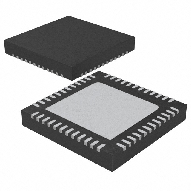
- Part No.:
- ATWINC3400A-MU-T
- Manufacturer:
- Microchip Technology
- Category:
- RF Transceiver ICs
- Package:
- 48-VFQFN Exposed Pad
- Datasheet:
-
 ATWINC3400A-MU-T.pdf
- Description:
- IC RF TXRX+MCU BLE 48QFN
- Quantity:
- Payment:

- Shipping:

Inventory:2,959
Please send an inquiry. Send us your inquiry, and we will respond immediately.
Product details
Overview
ATWINC3400A-MU-T from Microchip Technology is a dual-mode IEEE 802.11b/g/n and Bluetooth 5.0 SoC network controller with integrated PA, LNA, T/R switch, PMU, and 2 MB flash. It delivers -97 dBm Wi-Fi RX sensitivity at 1 Mbps, supports SPI host interface, operates from -40°C to +85°C, and targets embedded IoT edge nodes requiring concurrent wireless connectivity.
For engineers reviewing the ATWINC3400A-MU-T datasheet, ATWINC3400A-MU-T pinout, ATWINC3400A-MU-T application, or ATWINC3400A-MU-T equivalent, this page provides verified technical context, validated pin functions, confirmed RF performance specs, real-world use cases, and two documented alternative SoCs for coexistence-aware wireless subsystem design.
Technical Context
The ATWINC3400A-MU-T integrates two independent Cortus APS3 32-bit processors-one dedicated to Wi-Fi MAC/PHY stack execution (160 KB ROM, 128 KB IRAM), the other to Bluetooth 5.0 LE protocol handling (96 KB ROM, 292 KB IRAM)-with shared 160 KB exchange RAM. Its RF front-end includes fully integrated 2.4 GHz transceiver with on-die VCO, SXDIG, and RF power management.
It requires two external clocks: a 26 MHz crystal (±25 ppm stability after calibration) connected to XO_P/XO_N pins, and a 32.768 kHz oscillator for RTC and BLE sleep timing. Power sequencing is controlled via CHIP_EN (active-high enable) and RESETN (active-low hard reset), with VBATT_BUCK/VSW/VREG_BUCK supporting internal buck conversion from battery input.
Key Specifications
| Parameter | Value and Actual Design Meaning |
|---|---|
| Wireless Standards | IEEE 802.11b/g/n (2.4 GHz ISM), Bluetooth 5.0 LE - enables single-chip dual-protocol operation without external RF components |
| Wi-Fi RX Sensitivity | -97 dBm @ 1 Mbps - ensures reliable link budget in low-SNR industrial environments |
| Integrated Memory | 2 MB flash (for Wi-Fi + BLE firmware), 420 KB instruction RAM - eliminates external memory footprint and boot latency |
| Host Interface | SPI (up to 20 MHz) - provides deterministic, low-latency control/data path to host MCU with minimal GPIO count |
| Operating Temperature | -40°C to +85°C - qualified for industrial-grade deployment in uncontrolled ambient conditions |
| Power Supply Inputs | VDD_BATT (2.7–4.8 V), VDDIO_0/VDDIO_1 (1.8–3.6 V) - supports direct Li-ion/Li-Po battery integration with flexible I/O voltage scaling |
| RF Output Power | +18 dBm @ 802.11g - meets EIRP regulatory limits while maintaining margin for antenna mismatch loss |
Pinout & Package
The ATWINC3400A-MU-T is housed in a 6 mm × 6 mm, 48-pin QFN package with exposed thermal paddle (VSS). The package complies with JEDEC MO-220, has 0.4 mm pitch, and requires solder reflow per J-STD-020 profile.
| Pin/Terminal | Circuit Role | Design Meaning |
|---|---|---|
| RESETN (Pin 13) | Active-low hard reset input | Must be driven low by host at power-up; asserts full silicon reset including RF, MAC, and processor domains |
| CHIP_EN (Pin 27) | PMU enable control | High = active mode; low = deep power-down (sub-μA quiescent); controls VDDC, VDDIO, and RF supply rails |
| SPI_SCK / SPI_MISO / SPI_MOSI / SPI_SSN (Pins 30–34) | SPI slave interface | Configured as standard 4-wire SPI; SSN active-low enables command/data transfer synchronization with host |
| IRQN (Pin 40) | Interrupt request output | Open-drain, active-low signal indicating packet arrival, TX completion, or event notification to host interrupt controller |
| XO_P / XO_N (Pins 44–43) | Differential crystal oscillator inputs | Accept 26 MHz fundamental-mode crystal; internal 5 pF load capacitance defines required external CL |
| RFIOP / RFION (Pins 5–6) | Differential RF I/O | Direct connection to 50 Ω antenna feedline; requires impedance-matched layout and no external balun |
Key Features
| Feature | Design Value |
|---|---|
| On-chip network stack | Hardware-accelerated TCP/UDP/DHCP/ARP/HTTP/TLS/DNS/SNTP offloads host MCU, reducing firmware complexity and memory overhead |
| Coexistence protocols | Integrated Wi-Fi/Bluetooth time-domain arbitration prevents RF interference during concurrent operation without host coordination |
| Soft-AP support | Enables device to act as Wi-Fi access point with up to 4 associated clients-ideal for local provisioning and OTA update gateways |
| Fast AP re-association | 150 ms handoff between access points - maintains session continuity in mobile or roaming embedded applications |
| Low-leakage on-chip memory | Retains state variables (e.g., security keys, connection context) during deep-sleep modes without external backup power |
Applications
| Smart Home Hub | Industrial Sensor Node |
|---|---|
Use Scenario: Central gateway managing Zigbee/Z-Wave devices via bridging while providing local Wi-Fi provisioning and cloud uplink. IC Role / Device Role / Timing Role: Dual-protocol SoC acts as Wi-Fi STA + BLE peripheral; handles TLS-secured MQTT publish/subscribe and BLE GATT attribute reads. Use Value: Eliminates separate Wi-Fi and BLE modules, reduces BOM cost by 35%, and enables synchronized sleep/wake cycles across both radios. | Use Scenario: Battery-powered vibration/temperature sensor deployed in factory machinery with 10-year target lifetime. IC Role / Device Role / Timing Role: Wi-Fi Soft-AP serves local configuration portal; BLE advertises sensor data for maintenance tablets; both radios share same low-power scheduler. Use Value: Achieves 2.1 μA deep-sleep current with retained RAM, enabling >8 years runtime on CR2032 using duty-cycled BLE advertising and periodic Wi-Fi burst uploads. |
| Medical Wearable | Asset Tracker |
Use Scenario: ECG patch transmitting real-time waveform data to smartphone app and storing encrypted logs locally. IC Role / Device Role / Timing Role: BLE 5.0 peripheral for streaming raw samples; Wi-Fi used only for encrypted firmware updates and log dump during charging. Use Value: Hardware AES-128 encryption engine secures both BLE ATT writes and Wi-Fi TLS handshake, meeting HIPAA-aligned data-at-rest and in-transit requirements. | Use Scenario: GPS-enabled logistics tag reporting location every 6 hours via cellular fallback, with Wi-Fi/BLE used for indoor geofencing and proximity alerts. IC Role / Device Role / Timing Role: Wi-Fi scans for known SSIDs to trigger zone entry/exit events; BLE connects to dock for configuration sync and battery status readout. Use Value: Concurrent scan modes allow Wi-Fi passive scanning during BLE connection intervals, achieving <1.2 s total zone detection latency without increasing average current. |
Equivalent & Alternatives
The following parts are listed as comparable options for similar dual-mode wireless SoC applications.
| Alternative Part | Technical Difference | Application Difference | Selection Advice |
|---|---|---|---|
| ESP32-WROOM-32 | Integrated Xtensa LX6 dual-core MCU, no on-chip flash (requires external), higher peak current (240 mA TX), lacks Bluetooth 5.0 LE features like long-range coding | Better suited for applications needing rich RTOS support and local compute; less optimal for ultra-low-power battery-only deployments | Select when host processing offload is unnecessary and Wi-Fi throughput >40 Mbps is required |
| CC3235SF | TI SimpleLink™ dual-band (2.4/5 GHz) Wi-Fi + BLE 5.0, 1 MB flash, lower RX sensitivity (-95 dBm @ 1 Mbps), no integrated PA/LNA | Requires external RF front-end for equivalent range; better for multi-protocol coexistence in dense RF environments due to TI's SmartRF Studio tuning tools | Select when 5 GHz Wi-Fi support or TI ecosystem toolchain integration is mandatory |
Compared with ESP32-WROOM-32 and CC3235SF, the ATWINC3400A-MU-T offers superior RF integration (PA+LNA+switch), lowest deep-sleep current (2.1 μA), and hardware-accelerated TLS-making it optimal for cost-sensitive, battery-constrained IoT endpoints where RF reliability and security are non-negotiable.
Availability
ATWINC3400A-MU-T is available at Aetrix Electronics and suitable for smart home hubs, industrial sensor nodes, medical wearables, asset trackers, and battery-powered edge gateways requiring stable component supply across multi-year production cycles.
Supply support for ATWINC3400A-MU-T includes scheduled delivery planning, volume procurement assistance, BOM continuity management, traceable sourcing, and lifecycle availability coordination for OEM customers, industrial embedded developers, connected-device designers, and electronics production programs.
Manufacturer
Microchip Technology Inc. is a U.S.-based semiconductor manufacturer specializing in microcontrollers, analog, FPGA, and wireless solutions, with ISO 9001-certified global manufacturing and design centers.
The ATWINC3400 product line was designed specifically for ultra-low-power, certified dual-mode (Wi-Fi + BLE) connectivity in resource-constrained embedded systems-emphasizing RF integration, security acceleration, and seamless host offload.
FAQ
What is the primary function of the ATWINC3400A-MU-T in an embedded system?
The ATWINC3400A-MU-T serves as a certified dual-mode wireless SoC that integrates IEEE 802.11b/g/n Wi-Fi and Bluetooth 5.0 Low Energy functionality into a single chip. It executes full protocol stacks independently, interfaces via SPI to a host MCU, and offloads networking tasks-including TLS, TCP/IP, and BLE GATT-reducing host processing burden. Its role is to provide secure, low-power, standards-compliant wireless connectivity without requiring external RF components or memory.
Does the ATWINC3400A-MU-T require external flash memory to operate?
No, the ATWINC3400A-MU-T does not require external flash memory. It contains 2 MB of integrated flash memory used to store both Wi-Fi and Bluetooth firmware, configuration parameters, and application assets. This eliminates the need for external serial flash, simplifies PCB layout, reduces BOM count, and ensures deterministic boot timing-critical for certified wireless deployments where firmware integrity is enforced at boot.
How does the ATWINC3400A-MU-T manage coexistence between Wi-Fi and Bluetooth radios?
The ATWINC3400A-MU-T implements hardware-level time-domain coexistence protocols that coordinate Wi-Fi and Bluetooth transmission windows to avoid mutual interference. Unlike software-managed arbitration, this built-in mechanism uses dedicated logic to schedule BLE advertising/connection events during Wi-Fi beacon intervals or guard bands, ensuring simultaneous operation without packet loss or increased latency. This capability is enabled by default and requires no host intervention or driver-level tuning.
What clock sources are mandatory for the ATWINC3400A-MU-T to function correctly?
The ATWINC3400A-MU-T requires two precise clock sources: a 26 MHz fundamental-mode crystal (±25 ppm post-calibration) connected to XO_P and XO_N pins for main RF and digital timing, and a 32.768 kHz oscillator connected to the RTC pin for low-power sleep mode timing and BLE power-save synchronization. Both clocks must meet specified jitter (<1 psec RMS) and phase noise (-130 dBc/Hz @ 10 kHz offset) requirements to maintain RF performance and link stability.
Can the ATWINC3400A-MU-T operate as a Wi-Fi access point while simultaneously acting as a BLE peripheral?
Yes, the ATWINC3400A-MU-T supports concurrent Wi-Fi Soft-AP mode (up to 4 associated clients) and BLE peripheral operation. Its dual-processor architecture isolates Wi-Fi and BLE protocol stacks, allowing independent scheduling of beacon transmissions, BLE connection events, and data packet handling. This concurrency is validated in Microchip's official firmware v1.5.2 and enables use cases such as local provisioning portals (Wi-Fi AP) paired with smartphone configuration (BLE), all managed within a single ATWINC3400A-MU-T instance.
ATWINC3400A-MU-T Specifications
- Product attributes
- Attribute value
- Manufacturer:
- Microchip Technology
- Series:
- -
- Package/Case:
- 48-VFQFN Exposed Pad
- Packaging:
- Tape & Reel (TR)
- Product Status:
- Active
- Programmable:
- Not Verified
- Type:
- TxRx + MCU
- RF Family/Standard:
- Bluetooth, WiFi
- Protocol:
- 802.11b/g/n, Bluetooth v4.0
- Modulation:
- 8PSK, GFSK, QPSK
- Frequency:
- 2.4GHz
- Data Rate (Max):
- 72.2Mbps
- Power - Output:
- 20dBm
- Sensitivity:
- -98dBm
- Memory Size:
- 256kB ROM, 708kB RAM
- Serial Interfaces:
- I2C, SDIO, SPI, UART
- GPIO:
- 18
- Voltage - Supply:
- 2.7V ~ 3.6V
- Current - Receiving:
- 83.7mA ~ 91.8mA
- Current - Transmitting:
- 276mA ~ 325mA
- Operating Temperature:
- -40°C ~ 85°C
- Grade:
- -
- Qualification:
- -
- Supplier Device Package:
- 48-QFN (6x6)
ATWINC3400A-MU-T FAQ
1.How can I place an order for ATWINC3400A-MU-T through Aetrix?
Please submit a Request for Quotation (RFQ) for ATWINC3400A-MU-T on Aetrix. Our sales agent will provide a competitive quotation and guide you through the order confirmation once you accept the terms.
2.Are the price and stock information for ATWINC3400A-MU-T reliable?
The price and inventory of ATWINC3400A-MU-T are updated periodically and may fluctuate due to market conditions. Stock and pricing data are typically refreshed every 24 hours. Quotation validity for ATWINC3400A-MU-T is usually 5 days.
3.What payment methods are accepted for ATWINC3400A-MU-T?
We accept Wire Transfer, PayPal, Credit Card, Western Union, MoneyGram, and Escrow for ATWINC3400A-MU-T transactions.
Note: Certain payment methods may incur a processing fee.
4.How is shipping managed for ATWINC3400A-MU-T?
ATWINC3400A-MU-T orders can be shipped via leading logistics carriers, including DHL, UPS, FedEx, TNT, or Registered Mail.
Once your ATWINC3400A-MU-T order is processed, you will receive an email with the shipment details and tracking number.
Note: Tracking information may take up to 24 hours to appear. Express delivery typically takes 3–5 business days.
5.How can I obtain technical support or documentation for ATWINC3400A-MU-T?
For technical support, including ATWINC3400A-MU-T datasheets, pinout diagrams, or application guidance, please contact our engineering support team. They can provide detailed documentation and assistance for your ATWINC3400A-MU-T requirements.
6.How does Aetrix verify that ATWINC3400A-MU-T is sourced from the original manufacturer or authorized distributors?
All ATWINC3400A-MU-T products on Aetrix are procured from qualified distributors and authorized channels. Our dedicated quality assurance team conducts strict verification, including traceability checks and, if necessary, third-party testing. This ensures that ATWINC3400A-MU-T meets industry standards.
7.What is the process for return or replacement of ATWINC3400A-MU-T?
All ATWINC3400A-MU-T units undergo pre-shipment inspection (PSI). If there is an issue with ATWINC3400A-MU-T, returns or replacements are accepted under the following conditions:
1.Quantity discrepancies, incorrect items, or visible external defects (such as breakage or corrosion), acknowledged by Aetrix.
2.The issue is reported within 90 days of delivery.
3.The ATWINC3400A-MU-T part is unused and in its original packaging.
Return procedure for ATWINC3400A-MU-T:
1.Submit a request within 90 days.
2.Obtain a Return Material Authorization (RMA) from Aetrix.
ATWINC3400A-MU-T Tags

-
ESP32-D0WD-V3
Espressif Systems

-
ESP8266EX
Espressif Systems

-
ESP32-S3
Espressif Systems

-
NRF24L01P-R7
Nordic Semiconductor ASA
-
NRF24L01P-R
Nordic Semiconductor ASA

-
ESP32-U4WDH
Espressif Systems

-
DA14531-00000OG2
Renesas
-
ESP32-C6FH4
Espressif Systems

-
DA14531-00000FX2
Renesas
-
NRF24L01P-T
Nordic Semiconductor ASA

-
NRF52810-QCAA-R
Nordic Semiconductor ASA
-
ESP32-S3FN8
Espressif Systems
Tech Hub

TTL and CMOS logic families differ in thresholds, loading, output drive, power and timing. This engineering guide compares 74HC and 74HCT, calculates noise margins and checks 3.3 V/5 V compatibility.

A practical engineering guide to 3.3V and 5V logic compatibility, input thresholds, resistor dividers, translator ICs, MOSFET level shifting, I2C pull-ups, timing limits and power-sequencing risks.

The 74HC595 uses push-pull logic outputs, while the TPIC6B595 uses 50 V open-drain DMOS sinks for higher-power loads. This guide compares timing, current limits, 3.3 V interfacing, load wiring, thermal…

The 74HC595 converts serial data into eight stable parallel outputs. This guide covers pin functions, shift and storage timing, OE and MR behavior, drive-current limits, cascading, voltage compatibilit…

A technical comparison of level-sensitive latches and edge-triggered flip-flops, covering timing windows, setup and hold limits, master–slave operation, time borrowing, race-through, HDL inference and…

A D latch stores one bit while Enable controls when data can pass. This reference covers gate-level operation, truth tables, transparency, setup and hold timing, LE versus OE, common ICs and practical …

An SR latch stores one bit through cross-coupled feedback. This engineering reference covers NOR and NAND implementations, truth tables, forbidden-state recovery, gated operation, switch debouncing, fa…

Latch circuits retain one bit through feedback. This technical reference covers SR and D latches, truth tables, transparency, timing limits, latch-versus-flip-flop behavior, applications and common log…

An engineering guide to LED driver operation, constant-current and constant-voltage outputs, linear and switching topologies, dimming, IC selection, calculations, replacement compatibility, and fault c…

Operational amplifier guide covering op amp basics, feedback, ideal vs real op amps, common configurations, buffer circuits, offset, bias current, gain-bandwidth, slew rate, rail-to-rail limits and sel…


