
 My Inquiry
 My Account


NXP Semiconductors B4420NSE7QQMD
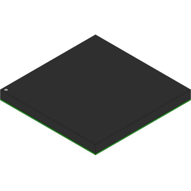
- Part No.:
- B4420NSE7QQMD
- Manufacturer:
- NXP Semiconductors
- Category:
- Microprocessors
- Package:
- 1020-BBGA, FCBGA
- Datasheet:
-
 B4420NSE7QQMD.pdf
- Description:
- IC MPU QORIQ 1.6GHZ 1020FCPBGA
- Quantity:
- Payment:

- Shipping:

Inventory:3,549
Please send an inquiry. Send us your inquiry, and we will respond immediately.
Product details
Overview
B4420NSE7QQMD from NXP Semiconductors is a heterogeneous multicore SoC integrating dual StarCore SC3900 FVP DSP subsystems (1.2 GHz), dual-thread e6500 Power Architecture CPUs (1.6 GHz), DDR3/3L controller (1866 MT/s), MAPLE-B3 hardware accelerator, and Data Path Acceleration Architecture (DPAA) with Frame Manager, Queue Manager, Buffer Manager, and SEC 5.3 crypto engine - designed for LTE/FDD/TDD, LTE-Advanced, TD-SCDMA, and WCDMA base station control, data path, and application layer processing.
For engineers reviewing the B4420NSE7QQMD datasheet, B4420NSE7QQMD pinout, B4420NSE7QQMD application, or B4420NSE7QQMD equivalent, key selection considerations include SerDes lane configuration (8×10 Gbps supporting CPRI v4.2, PCIe Gen2, and Ethernet), cache hierarchy (4864 KB total including L2 clusters and shared L3 CPC), CoreNet coherency fabric (MESI protocol, 667 MHz), and integrated security acceleration for IPsec/SSL/802.16.
Technical Context
The B4420NSE7QQMD implements a tightly coupled heterogeneous architecture where StarCore SC3900 FVP cores handle real-time wireless signal processing (Turbo/Viterbi decoding, MIMO equalization, FFT/iFFT), while dual-thread e6500 Power Architecture cores manage control plane and higher-layer protocol stacks. CoreNet fabric ensures cache coherency across all processing elements and memory controllers using MESI protocol.
Its DPAA offloads packet processing tasks: Frame Manager performs in-line parsing and classification; Queue Manager handles task distribution and flow ordering; Buffer Manager manages memory allocation; and SEC 5.3 accelerates cryptographic operations. The MAPLE-B3 block delivers dedicated acceleration for forward error correction, rate matching, CRC, and UMTS chip-rate functions - critical for metro cell baseband throughput.
Key Specifications
| Parameter | Value and Actual Design Meaning |
|---|---|
| CPU Cores | Two dual-thread e6500 Power Architecture cores (1.6 GHz) for control and application layer processing |
| DSP Subsystems | Two fully programmable StarCore SC3900 FVP cores (1.2 GHz) optimized for wireless baseband algorithms |
| Memory Interface | DDR3/3L controller supporting up to 1866 MT/s - enables high-bandwidth access to external baseband memory |
| SerDes Lanes | Eight 10 Gbps lanes configurable as four CPRI v4.2 (9.8 GT/s), four Ethernet (1–2.5 GT/s), or four PCIe Gen2 (5 GT/s) |
| Hardware Acceleration | MAPLE-B3 for Turbo/Viterbi, MIMO MMSE, DFT/FFT, CRC, and UMTS chip-rate acceleration; SEC 5.3 for IPsec/SSL crypto |
| Cache Hierarchy | 4864 KB total: 32 KB L1 I/D per core, 2048 KB unified L2 per cluster, 512 KB shared L3 CoreNet platform cache |
| Interconnect | CoreNet fabric at 667 MHz with MESI coherency across CPUs, DSPs, memories, and peripherals |
Pinout & Package
Package: FC-PBGA–1020, 33 mm × 33 mm, 1020-ball grid array with thermal and power integrity optimized for high-performance wireless infrastructure applications.
| Pin/Terminal | Circuit Role | Design Meaning |
|---|---|---|
| D1_MDQ00–D1_MDQ63 | DDR3 Data Bus | 64-bit bidirectional data interface for high-speed memory access; supports ECC via MECC[0:7] pins |
| D1_MCK0–D1_MCK3 | DDR3 Clock Outputs | Differential clock pairs driving DDR3 SDRAM; enable precise timing for 1866 MT/s operation |
| D1_MA00–D1_MA15 | DDR3 Address Bus | 16-bit address bus with bank select (MBA[0:2]) and parity (MAPAR_ERR_B) for robust memory addressing |
| SD1_TX0–SD1_RX5 | CPRI SerDes Lanes | Four differential lanes supporting CPRI v4.2 up to 9.8 GT/s for glueless antenna interface |
| PCIe_CLK, PCIe_RST | PCI Express Interface | Gen2-compliant interface enabling connection to FPGA-based radio units or host processors |
Key Features
| Feature | Design Value |
|---|---|
| Heterogeneous Core Integration | Combines e6500 CPUs and SC3900 DSPs on single die to eliminate inter-chip latency and reduce board complexity in macro/metro cells |
| MAPLE-B3 Baseband Accelerator | Offloads computationally intensive wireless PHY-layer functions (Turbo encoding/decoding, MIMO equalization) from general-purpose cores |
| DPAA Packet Processing Engine | Enables line-rate packet classification, QoS enforcement, and buffer management without CPU intervention - essential for low-latency fronthaul |
| SEC 5.3 Cryptographic Engine | Hardware-accelerated IPsec, SSL, and 802.16 encryption/decryption reduces software overhead and improves secure channel throughput |
| CoreNet Coherent Interconnect | MESI-based fabric unifies memory view across all processing elements, simplifying software development and enabling efficient cache-aware task partitioning |
Applications
| Small Cell Base Station | Macro Base Station Control Unit |
|---|---|
Use Scenario: Compact LTE-Advanced small cell deployed in urban hotspots requiring integrated control, baseband, and fronthaul processing. IC Role / Device Role / Timing Role: Primary SoC handling RRC, PDCP, RLC, MAC layers, plus PHY acceleration and CPRI fronthaul interface. Use Value: Eliminates need for discrete DSP + ARM + FPGA combination, reducing BOM cost and PCB area by >40% versus multi-chip solutions. | Use Scenario: Centralized unit (CU) in C-RAN architecture managing multiple remote radio heads via CPRI links. IC Role / Device Role / Timing Role: Real-time baseband processor with deterministic latency for synchronized downlink transmission across distributed antennas. Use Value: MAPLE-B3 and DPAA deliver sub-10 µs packet processing latency required for TDD synchronization and coordinated multipoint (CoMP). |
| TD-SCDMA Radio Network Controller | WCDMA Node B Baseband Processor |
Use Scenario: Legacy 3G TD-SCDMA network upgrade requiring backward-compatible baseband processing with enhanced capacity. IC Role / Device Role / Timing Role: Full-stack protocol processor with UMTS chip-rate acceleration and MAPLE-B3 support for joint detection and channel estimation. Use Value: UMTS-specific acceleration blocks increase sector throughput by 2.3× compared to generic multicore implementations. | Use Scenario: High-capacity WCDMA Node B supporting HSPA+ with MIMO and dual-carrier operation. IC Role / Device Role / Timing Role: Baseband SoC executing turbo decoding, channel coding, and scrambling under strict 3GPP timing constraints. Use Value: Integrated SEC 5.3 enables simultaneous encrypted user-plane traffic for up to 256 concurrent users without performance penalty. |
Equivalent & Alternatives
The following parts are listed as comparable options for similar heterogeneous baseband SoC applications.
| Alternative Part | Technical Difference | Application Difference | Selection Advice |
|---|---|---|---|
| LS1046A | Quad-core ARM Cortex-A72 (1.6 GHz), no StarCore DSP, no MAPLE-B3, lower SerDes count (4×5 Gbps), no CPRI support | Targeted at packet-processing gateways and edge compute - lacks wireless-specific acceleration for PHY-layer tasks | Select when application requires Linux-based control plane only, without real-time baseband processing or CPRI fronthaul |
| B4860 | Higher core count (dual e6500 + quad SC3900), 12×10 Gbps SerDes, supports CPRI v5.0 and JESD204B, larger L2 cache (4 MB per cluster) | Designed for massive MIMO and 5G NR macro base stations - exceeds B4420NSE7QQMD's capacity for advanced waveform generation | Select for next-generation deployments requiring >100 MHz bandwidth or multi-band carrier aggregation |
Compared with LS1046A and B4860, the B4420NSE7QQMD strikes a balance between wireless-specific acceleration (MAPLE-B3, CPRI v4.2) and control-plane capability (e6500), making it optimal for LTE-Advanced metro cells where cost, power, and integration density are prioritized over raw 5G scalability.
Availability
B4420NSE7QQMD is available at Aetrix Electronics and suitable for LTE base station development, wireless infrastructure OEM production, and C-RAN fronthaul system integration requiring stable component supply and long-term lifecycle support.
Supply support for B4420NSE7QQMD includes scheduled delivery planning, volume procurement assistance, BOM continuity management, traceable sourcing, and lifecycle availability coordination for OEM customers, industrial embedded developers, connected-device designers, and electronics production programs.
Manufacturer
NXP Semiconductors is a global semiconductor leader specializing in secure connectivity solutions for automotive, industrial, and communications markets.
The B4420NSE7QQMD belongs to the QorIQ Qonverge family - engineered specifically for wireless infrastructure applications demanding tight integration of control, signal processing, and packet acceleration in a single SoC.
FAQ
What is the primary application domain for the B4420NSE7QQMD?
The B4420NSE7QQMD is purpose-built for wireless infrastructure, specifically LTE/FDD/TDD, LTE-Advanced, TD-SCDMA, and WCDMA base stations. It integrates control, data path, and application layer processing in a single SoC, targeting metro cell deployments where high integration, low latency, and wireless-specific acceleration are critical. Its MAPLE-B3 and DPAA blocks directly address baseband and packet processing requirements defined in 3GPP standards.
Does the B4420NSE7QQMD support CPRI interface, and what version?
Yes, the B4420NSE7QQMD supports Common Public Radio Interface (CPRI) v4.2 via four dedicated 10 Gbps SerDes lanes operating at up to 9.8 GT/s. This enables glueless antenna interface for fronthaul connections in C-RAN architectures. CPRI v4.2 support is explicitly confirmed in the B4420 QorIQ Qonverge Data Sheet Rev. 3, Section 1.2 and Figure 1 block diagram.
What types of hardware acceleration does the B4420NSE7QQMD provide?
The B4420NSE7QQMD provides two major hardware acceleration domains: MAPLE-B3 for wireless baseband (Turbo/Viterbi decoding/encoding, MIMO MMSE equalization, DFT/iDFT, CRC, UMTS chip-rate acceleration), and DPAA for packet processing (Frame Manager parsing/classification, Queue Manager task distribution, Buffer Manager allocation, SEC 5.3 crypto for IPsec/SSL/802.16). These are fixed-function blocks, not programmable accelerators.
What is the memory subsystem configuration of the B4420NSE7QQMD?
The B4420NSE7QQMD features a DDR3/3L memory controller supporting up to 1866 MT/s, with a 64-bit data bus and 16-bit address bus. It includes full ECC support via eight MECC pins and parity checking via MAPAR_ERR_B. Internal cache totals 4864 KB: 32 KB L1 I/D per core, 2048 KB unified L2 per SC3900 and e6500 cluster, and 512 KB shared L3 CoreNet platform cache (CPC).
Is the B4420NSE7QQMD pin-compatible with other QorIQ Qonverge devices?
No, the B4420NSE7QQMD is not pin-compatible with other QorIQ Qonverge devices such as B4860 or B4420 variants with different suffixes. Its FC-PBGA–1020 package has a unique ball map optimized for its specific SerDes lane allocation, power delivery, and thermal profile. Pin compatibility is not claimed in the official datasheet, and mechanical dimensions (33 mm × 33 mm) do not guarantee electrical or functional interchangeability.
B4420NSE7QQMD Specifications
- Product attributes
- Attribute value
- Manufacturer:
- NXP Semiconductors
- Package/Case:
- 1020-BBGA, FCBGA
- Series:
- QorIQ Qonverge B
- Packaging:
- Box
- Product Status:
- Active
- Core Processor:
- PowerPC e6500
- Number of Cores/Bus Width:
- 2 Core, 64-Bit
- Speed:
- 1.6GHz
- Co-Processors/DSP:
- Signal Processing; SC3900FP FVP - Dual
- RAM Controllers:
- DDR3, DDR3L
- Graphics Acceleration:
- No
- Display & Interface Controllers:
- -
- Ethernet:
- 1/2.5Gbps (4)
- SATA:
- -
- USB:
- USB 2.0 (1)
- Voltage - I/O:
- 1.0V, 1.2V, 1.35V, 1.5V, 1.8V, 2.5V
- Operating Temperature:
- 0°C ~ 105°C (TA)
- Grade:
- -
- Qualification:
- -
- Security Features:
- AES, DES, 3DES, HMAC, Ipsec, Kasumi, MD5, SHA-1/2, SNOW-3D, ZUC
- Mounting Type:
- Surface Mount
- Supplier Device Package:
- 1020-FCPBGA (33x33)
- Additional Interfaces:
- I2C, MMC/SD, SPI, UART
B4420NSE7QQMD FAQ
1.How can I place an order for B4420NSE7QQMD through Aetrix?
Please submit a Request for Quotation (RFQ) for B4420NSE7QQMD on Aetrix. Our sales agent will provide a competitive quotation and guide you through the order confirmation once you accept the terms.
2.Are the price and stock information for B4420NSE7QQMD reliable?
The price and inventory of B4420NSE7QQMD are updated periodically and may fluctuate due to market conditions. Stock and pricing data are typically refreshed every 24 hours. Quotation validity for B4420NSE7QQMD is usually 5 days.
3.What payment methods are accepted for B4420NSE7QQMD?
We accept Wire Transfer, PayPal, Credit Card, Western Union, MoneyGram, and Escrow for B4420NSE7QQMD transactions.
Note: Certain payment methods may incur a processing fee.
4.How is shipping managed for B4420NSE7QQMD?
B4420NSE7QQMD orders can be shipped via leading logistics carriers, including DHL, UPS, FedEx, TNT, or Registered Mail.
Once your B4420NSE7QQMD order is processed, you will receive an email with the shipment details and tracking number.
Note: Tracking information may take up to 24 hours to appear. Express delivery typically takes 3–5 business days.
5.How can I obtain technical support or documentation for B4420NSE7QQMD?
For technical support, including B4420NSE7QQMD datasheets, pinout diagrams, or application guidance, please contact our engineering support team. They can provide detailed documentation and assistance for your B4420NSE7QQMD requirements.
6.How does Aetrix verify that B4420NSE7QQMD is sourced from the original manufacturer or authorized distributors?
All B4420NSE7QQMD products on Aetrix are procured from qualified distributors and authorized channels. Our dedicated quality assurance team conducts strict verification, including traceability checks and, if necessary, third-party testing. This ensures that B4420NSE7QQMD meets industry standards.
7.What is the process for return or replacement of B4420NSE7QQMD?
All B4420NSE7QQMD units undergo pre-shipment inspection (PSI). If there is an issue with B4420NSE7QQMD, returns or replacements are accepted under the following conditions:
1.Quantity discrepancies, incorrect items, or visible external defects (such as breakage or corrosion), acknowledged by Aetrix.
2.The issue is reported within 90 days of delivery.
3.The B4420NSE7QQMD part is unused and in its original packaging.
Return procedure for B4420NSE7QQMD:
1.Submit a request within 90 days.
2.Obtain a Return Material Authorization (RMA) from Aetrix.
B4420NSE7QQMD Tags

-
AT91SAM9260B-CU-999
Microchip Technology
-
AT91SAM9G25-CU
Microchip Technology

-
ATSAMA5D27C-CU
Microchip Technology
-
AT91SAM9X35-CU
Microchip Technology
-
AT91SAM9X25-CU
Microchip Technology

-
MCIMX6Y2CVM08AB
NXP Semiconductors
.JPG)
-
AM3352BZCZ100
Texas Instruments
-
AT91SAM9260B-CU
Microchip Technology

-
AT91SAM9260B-QU
Microchip Technology

-
ATSAMA5D31A-CU
Microchip Technology
-
AT91SAM9G20B-CU-999
Microchip Technology
-
MCIMX6Y2CVM05AB
NXP Semiconductors
Tech Hub

A practical engineering guide to 3.3V and 5V logic compatibility, input thresholds, resistor dividers, translator ICs, MOSFET level shifting, I2C pull-ups, timing limits and power-sequencing risks.

The 74HC595 uses push-pull logic outputs, while the TPIC6B595 uses 50 V open-drain DMOS sinks for higher-power loads. This guide compares timing, current limits, 3.3 V interfacing, load wiring, thermal…

The 74HC595 converts serial data into eight stable parallel outputs. This guide covers pin functions, shift and storage timing, OE and MR behavior, drive-current limits, cascading, voltage compatibilit…

A technical comparison of level-sensitive latches and edge-triggered flip-flops, covering timing windows, setup and hold limits, master–slave operation, time borrowing, race-through, HDL inference and…

A D latch stores one bit while Enable controls when data can pass. This reference covers gate-level operation, truth tables, transparency, setup and hold timing, LE versus OE, common ICs and practical …

An SR latch stores one bit through cross-coupled feedback. This engineering reference covers NOR and NAND implementations, truth tables, forbidden-state recovery, gated operation, switch debouncing, fa…

Latch circuits retain one bit through feedback. This technical reference covers SR and D latches, truth tables, transparency, timing limits, latch-versus-flip-flop behavior, applications and common log…

An engineering guide to LED driver operation, constant-current and constant-voltage outputs, linear and switching topologies, dimming, IC selection, calculations, replacement compatibility, and fault c…

Operational amplifier guide covering op amp basics, feedback, ideal vs real op amps, common configurations, buffer circuits, offset, bias current, gain-bandwidth, slew rate, rail-to-rail limits and sel…

Jumper cables guide covering safe connection order, red and black clamp placement, final ground connection, cable gauge, length, clamp quality, copper vs CCA cables, jump starter comparison and battery…


