
 My Inquiry
 My Account


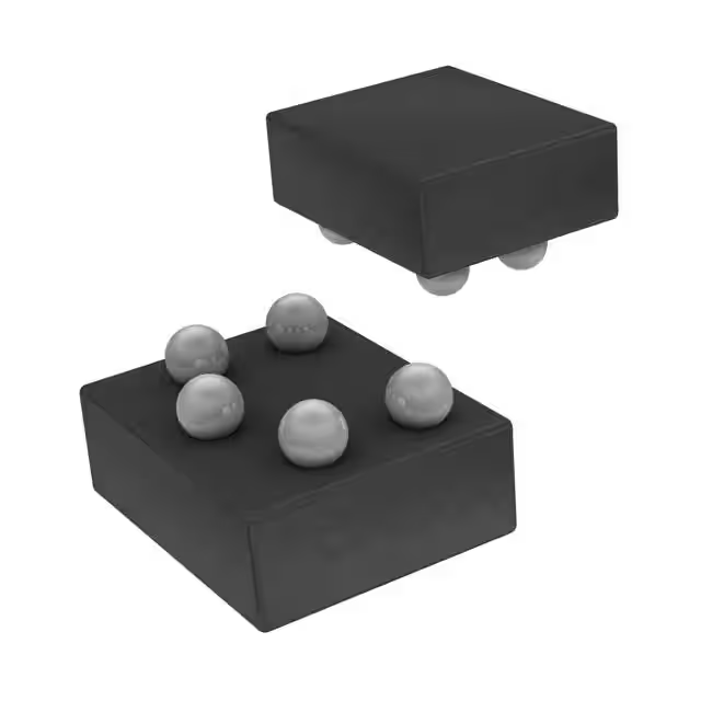
STMicroelectronics BAL-CW1250D3
- Part No.:
- BAL-CW1250D3
- Manufacturer:
- STMicroelectronics
- Category:
- Balun
- Package:
- 5-UFBGA, FCBGA
- Datasheet:
-
 BAL-CW1250D3.pdf
- Description:
- BALUN 2.4GHZ-2.5GHZ 5UFBGA FCBGA
- Quantity:
- Payment:

- Shipping:

Inventory:4,904
Please send an inquiry. Send us your inquiry, and we will respond immediately.
Product details
Overview
BAL-CW1250D3 from STMicroelectronics is a 50 Ω nominal input flip-chip balun with integrated harmonic filter, designed specifically for differential conversion in 2.4–2.5 GHz WLAN RF front-ends interfacing ST-Ericsson CW1250/CW1150/CW1260/CW1160 transceivers. It delivers 0.97 dB typical insertion loss, ±1 dB amplitude imbalance, and ±10° phase imbalance across its bandwidth, enabling high-fidelity single-ended to differential signal transformation in compact Wi-Fi modules.
For engineers reviewing the BAL-CW1250D3 datasheet, BAL-CW1250D3 pinout, BAL-CW1250D3 application, or BAL-CW1250D3 equivalent, key selection criteria include its 2.4–2.5 GHz bandwidth, integrated matching network for CW-series ICs, DC-blocking on SE input, <550 µm profile after reflow, and flip-chip bump layout compatibility with 0.4 mm pitch land patterns.
Technical Context
This balun implements a passive impedance transformation using STMicroelectronics' IPD (Integrated Passive Device) technology on non-conductive glass substrate, enabling optimized RF performance and harmonic suppression without external components. Its design embeds a conjugate-matched 50 Ω single-ended input and differential output matched to the CW1250 family's internal transceiver interface.
The device integrates a second-harmonic filter achieving –19 dB attenuation at 2f₀, supports 24 dBm average RF input power, and features DC blocking on the single-ended RF input terminal-eliminating need for external AC coupling capacitors in the signal path.
Key Specifications
| Parameter | Value and Actual Design Meaning |
|---|---|
| Frequency Range | 2400–2500 MHz: Full operational bandwidth for IEEE 802.11b/g/n 2.4 GHz WLAN channels. |
| Insertion Loss | 0.97 dB typ: Low signal attenuation preserves PA/LNA SNR and system EVM in Wi-Fi RF chains. |
| Amplitude Imbalance | ±1 dB max: Ensures balanced I/Q signal integrity critical for OFDM modulation fidelity. |
| Phase Imbalance | ±10° max: Maintains orthogonal signal relationship required for quadrature demodulation accuracy. |
| 2nd Harmonic Attenuation | –19 dB: Integrated filtering reduces out-of-band emissions without discrete LC filters. |
| Input Impedance | 50 Ω nominal: Direct match to standard RF PCB traces and test equipment interfaces. |
| Package Size | 0.94 × 1.15 mm die area (<1.2 mm²): Enables ultra-dense RF module layouts in mobile and IoT designs. |
Pinout & Package
Flip-Chip package with 5 solder bumps on non-conductive glass substrate; total height ≤ 0.69 mm after reflow; UL94 V0 epoxy; RoHS-compliant and ECOPACK® certified.
| Pin/Terminal | Circuit Role | Design Meaning |
|---|---|---|
| SE (Bump A) | Single-ended RF input | DC-blocked input port accepting 50 Ω source; connects directly to transceiver RFOUT or PA driver. |
| GND (Bump B) | Ground reference | RF ground return path for balun core; must be connected to low-inductance ground plane under die. |
| VCC (Bump C) | Supply bypass terminal | Not powered; used as DC tie point for internal bias network-requires local 100 nF decoupling to GND. |
| DIFF+ (Bump 2) | Differential output positive | Matches CW1250-series differential input impedance; connects to transceiver I+ or Q+ path. |
| DIFF– (Bump 1) | Differential output negative | Complementary output to DIFF+; maintains 100 Ω differential impedance with matched trace routing. |
Key Features
| Feature | Design Value |
|---|---|
| Integrated matching network | Eliminates ≥3 external matching components per RF path, reducing BOM count and layout area by >1.5 mm². |
| DC blocking on SE input | Removes need for series AC-coupling capacitor, simplifying layout and avoiding DC bias shift in PA/LNA stages. |
| IPD-on-glass construction | Delivers stable Q-factor and low parasitic coupling vs. silicon-based passives, critical for 2.4 GHz phase linearity. |
| Harmonic filtering | –19 dB 2f₀ suppression enables direct connection to PA output without added bandpass filtering. |
Applications
| Wi-Fi 2.4 GHz Transceiver Interface | Compact WLAN Module Design |
|---|---|
Use Scenario: Interfacing CW1250 RFIC to external PA/LNA in dual-band 2.4/5 GHz front-end modules. IC Role / Device Role / Timing Role: Single-ended to differential balun with embedded matching and harmonic filtering. Use Value: Reduces component count by 4 parts per RF chain while maintaining EVM <3% at 54 Mbps OFDM. | Use Scenario: Space-constrained IoT access point PCB where RF section occupies <8 mm². IC Role / Device Role / Timing Role: Miniaturized RF interface component enabling sub-1 mm² balun footprint. Use Value: Enables full 2.4 GHz WLAN RF path within 1.2 mm² area-critical for wearable and sensor hub designs. |
| ST-Ericsson CW-Series Reference Design | Low-Profile Mobile Wi-Fi Antenna Coupling |
Use Scenario: Production implementation on CW1250 evaluation board (REF-CW1250-DB). IC Role / Device Role / Timing Role: Factory-validated balun matching network specified in ST AN2348. Use Value: Guarantees return loss >21 dB and phase balance within ±8° across production lots. | Use Scenario: Direct coupling between antenna switch and transceiver in slim smartphone bezel. IC Role / Device Role / Timing Role: Ultra-low-profile (<550 µm) balun enabling mechanical clearance under metal frame. Use Value: Allows 0.55 mm maximum Z-height stack-up without compromising 2.4 GHz radiation efficiency. |
Availability
BAL-CW1250D3 is available at Aetrix Electronics and suitable for Wi-Fi 2.4 GHz transceiver interfaces, compact WLAN module designs, and ST-Ericsson CW-series reference implementations requiring stable component supply and consistent RF performance across volume production.
Supply support for BAL-CW1250D3 includes scheduled delivery planning, volume procurement assistance, BOM continuity management, traceable sourcing, and lifecycle availability coordination for OEM customers, industrial embedded developers, connected-device designers, and electronics production programs.
Manufacturer
STMicroelectronics is a global semiconductor leader headquartered in Geneva, Switzerland, designing and manufacturing analog, MEMS, power, and microcontroller solutions for automotive, industrial, and consumer markets.
BAL-CW1250D3 belongs to ST's IPD-based RF passive portfolio, engineered specifically to replace discrete balun + matching networks in ST-Ericsson and compatible WLAN transceivers-targeting miniaturization and RF repeatability in mass-produced Wi-Fi modules.
FAQ
What is the recommended PCB land pattern for BAL-CW1250D3?
The manufacturer specifies a non-solder-mask-defined (NSMD) footprint with 0.4 mm X-pitch and 0.76 mm Y-pitch bump spacing. Recommended pad dimensions are 0.255 mm diameter copper pads with 0.3 mm solder mask opening, aligned to Figure 14 in DocID024678 Rev 2. Stencil aperture should be 3 mils thick with 0.25 mm openings for optimal flip-chip reflow yield.
Does BAL-CW1250D3 require external DC blocking capacitors?
No. The SE input terminal includes integrated DC blocking, allowing direct connection to RF output pins of CW1250-series transceivers without series capacitors. External DC blocking is only needed if the source stage lacks proper bias isolation-verified via S11 measurement below 100 MHz.
Can BAL-CW1250D3 be used with non-CW-series RFICs?
It is not recommended. The differential output impedance and phase response are optimized for CW1250/CW1150/CW1260/CW1160 transceivers. Using it with other ICs may result in >–15 dB differential return loss and degraded EVM due to mismatched load termination and harmonic tuning.
What is the maximum RF input power rating for continuous operation?
The absolute maximum average RF input power is 24 dBm (250 mW), per Table 1 in the datasheet. Derating is required above +70 °C ambient; at 85 °C, maximum safe average power drops to 21 dBm to maintain reliability and prevent substrate heating-induced parameter drift.
BAL-CW1250D3 Specifications
- Product attributes
- Attribute value
- Manufacturer:
- STMicroelectronics
- Series:
- -
- Package/Case:
- 5-UFBGA, FCBGA
- Packaging:
- Tape & Reel (TR)
- Product Status:
- Obsolete
- Frequency Range:
- 2.4GHz ~ 2.5GHz
- Impedance - Unbalanced/Balanced:
- 50 / -Ohm
- Phase Difference:
- 10°
- Insertion Loss (Max):
- 0.97dB
- Return Loss (Min):
- 21dB
- Mounting Type:
- Surface Mount
BAL-CW1250D3 FAQ
1.How can I place an order for BAL-CW1250D3 through Aetrix?
Please submit a Request for Quotation (RFQ) for BAL-CW1250D3 on Aetrix. Our sales agent will provide a competitive quotation and guide you through the order confirmation once you accept the terms.
2.Are the price and stock information for BAL-CW1250D3 reliable?
The price and inventory of BAL-CW1250D3 are updated periodically and may fluctuate due to market conditions. Stock and pricing data are typically refreshed every 24 hours. Quotation validity for BAL-CW1250D3 is usually 5 days.
3.What payment methods are accepted for BAL-CW1250D3?
We accept Wire Transfer, PayPal, Credit Card, Western Union, MoneyGram, and Escrow for BAL-CW1250D3 transactions.
Note: Certain payment methods may incur a processing fee.
4.How is shipping managed for BAL-CW1250D3?
BAL-CW1250D3 orders can be shipped via leading logistics carriers, including DHL, UPS, FedEx, TNT, or Registered Mail.
Once your BAL-CW1250D3 order is processed, you will receive an email with the shipment details and tracking number.
Note: Tracking information may take up to 24 hours to appear. Express delivery typically takes 3–5 business days.
5.How can I obtain technical support or documentation for BAL-CW1250D3?
For technical support, including BAL-CW1250D3 datasheets, pinout diagrams, or application guidance, please contact our engineering support team. They can provide detailed documentation and assistance for your BAL-CW1250D3 requirements.
6.How does Aetrix verify that BAL-CW1250D3 is sourced from the original manufacturer or authorized distributors?
All BAL-CW1250D3 products on Aetrix are procured from qualified distributors and authorized channels. Our dedicated quality assurance team conducts strict verification, including traceability checks and, if necessary, third-party testing. This ensures that BAL-CW1250D3 meets industry standards.
7.What is the process for return or replacement of BAL-CW1250D3?
All BAL-CW1250D3 units undergo pre-shipment inspection (PSI). If there is an issue with BAL-CW1250D3, returns or replacements are accepted under the following conditions:
1.Quantity discrepancies, incorrect items, or visible external defects (such as breakage or corrosion), acknowledged by Aetrix.
2.The issue is reported within 90 days of delivery.
3.The BAL-CW1250D3 part is unused and in its original packaging.
Return procedure for BAL-CW1250D3:
1.Submit a request within 90 days.
2.Obtain a Return Material Authorization (RMA) from Aetrix.
BAL-CW1250D3 Tags

-
2450BL15B0100001E
Johanson Technology Inc.
-
0900BL15D0050001E
Johanson Technology Inc.
-
0900PC16J0042001E
Johanson Technology Inc.
-
2450BM15A0002001E
Johanson Technology Inc.
-
2450BM14G0011001T
Johanson Technology Inc.
-
BD0810N50100AHF
TTM Technologies, Inc.
-
1720BL15B0050001E
Johanson Technology Inc.
-
0900PC15A0036001E
Johanson Technology Inc.
-
0868BM15C0001001E
Johanson Technology Inc.
-
0915BM15A0001001E
Johanson Technology Inc.
-
HHM1776B3
TDK Corporation
-
2450BM14E0003001T
Johanson Technology Inc.
Tech Hub

A practical engineering guide to 3.3V and 5V logic compatibility, input thresholds, resistor dividers, translator ICs, MOSFET level shifting, I2C pull-ups, timing limits and power-sequencing risks.

The 74HC595 uses push-pull logic outputs, while the TPIC6B595 uses 50 V open-drain DMOS sinks for higher-power loads. This guide compares timing, current limits, 3.3 V interfacing, load wiring, thermal…

The 74HC595 converts serial data into eight stable parallel outputs. This guide covers pin functions, shift and storage timing, OE and MR behavior, drive-current limits, cascading, voltage compatibilit…

A technical comparison of level-sensitive latches and edge-triggered flip-flops, covering timing windows, setup and hold limits, master–slave operation, time borrowing, race-through, HDL inference and…

A D latch stores one bit while Enable controls when data can pass. This reference covers gate-level operation, truth tables, transparency, setup and hold timing, LE versus OE, common ICs and practical …

An SR latch stores one bit through cross-coupled feedback. This engineering reference covers NOR and NAND implementations, truth tables, forbidden-state recovery, gated operation, switch debouncing, fa…

Latch circuits retain one bit through feedback. This technical reference covers SR and D latches, truth tables, transparency, timing limits, latch-versus-flip-flop behavior, applications and common log…

An engineering guide to LED driver operation, constant-current and constant-voltage outputs, linear and switching topologies, dimming, IC selection, calculations, replacement compatibility, and fault c…

Operational amplifier guide covering op amp basics, feedback, ideal vs real op amps, common configurations, buffer circuits, offset, bias current, gain-bandwidth, slew rate, rail-to-rail limits and sel…

Jumper cables guide covering safe connection order, red and black clamp placement, final ground connection, cable gauge, length, clamp quality, copper vs CCA cables, jump starter comparison and battery…


