
 My Inquiry
 My Account


STMicroelectronics BALFLB-WL-07D3
- Part No.:
- BALFLB-WL-07D3
- Manufacturer:
- STMicroelectronics
- Category:
- Balun
- Package:
- 8-WFBGA, CSPBGA
- Datasheet:
-
 BALFLB-WL-07D3.pdf
- Description:
- BALUN,FILTERING AND MATCHING OF
- Quantity:
- Payment:

- Shipping:

Inventory:3,831
Please send an inquiry. Send us your inquiry, and we will respond immediately.
Product details
Overview
BALFLB-WL-07D3 from STMicroelectronics is an ultra-miniature integrated balun + Tx harmonic filter optimized for BGA-packaged STM32WL sub-GHz wireless microcontrollers in high-power mode. It provides 50 Ω conjugate-matched differential Rx balun input, 50 Ω antenna-side Tx/Rx impedance, deep harmonic rejection (≥45 dB at 2f₀), ≤2.05 dB typical Rx insertion loss, and ≤2.15 dB Tx insertion loss across 470–510 MHz - enabling LoRa®, (G)FSK, and BPSK LPWAN radio solutions on 4-layer PCBs.
For engineers reviewing the BALFLB-WL-07D3 datasheet, BALFLB-WL-07D3 pinout, BALFLB-WL-07D3 application, or BALFLB-WL-07D3 equivalent, key selection criteria include its 8-bump CSPG package footprint, RF performance validation for STM32WL RFO_HP and RFI_P/N_out interfaces, harmonic suppression up to 10f₀, and compatibility with ECOPACK2-compliant assembly processes including 240–245 °C reflow peak and 3-mil stencil design.
Technical Context
This device integrates three RF functions in a single IPD-on-glass die: a differential-to-single-ended Rx balun matched to STM32WL's RFI_P/N_out pins, a Tx filter with 50 Ω input/output matched to RFO_in/RFO_out, and a wideband harmonic rejection network targeting 2f₀–10f₀. All functions are co-optimized for operation in the 470–510 MHz band under high-power transmit conditions.
The balun delivers <±0.3 dB amplitude imbalance and <±1.9° phase imbalance across band, while the Tx filter achieves ≥45 dB attenuation at 2f₀ and ≥21 dB at 10f₀. Impedance matching is fixed: ZRX = conjugate match to STM32WL Rx port, ZTX = 50 Ω to RFO_HP, and both antenna ports are 50 Ω nominal.
Key Specifications
| Parameter | Value and Actual Design Meaning |
|---|---|
| Frequency range | 470–510 MHz - validated operating band for STM32WL high-power sub-GHz transmission and reception |
| Rx insertion loss (ILRX) | 1.80–2.05 dB typ - low-loss signal path from STM32WL differential RFI_P/N_out to single-ended RFI_in |
| Tx insertion loss (ILTX) | 1.75–2.15 dB typ - minimal power loss between STM32WL RFO_HP and antenna |
| Harmonic rejection (2f₀) | 45–48 dB - suppresses second harmonic energy to meet ETSI/FCC spectral mask requirements |
| Return loss (Rx/Tx antenna side) | 16–22 dB - ensures >96% power transfer efficiency at antenna interface under matched 50 Ω load |
| Package height | ≤630 μm after reflow - enables ultra-low-profile integration in space-constrained IoT modules |
| ESD rating (HBM) | 2000 V - robustness against handling-induced electrostatic discharge during PCB assembly |
Pinout & Package
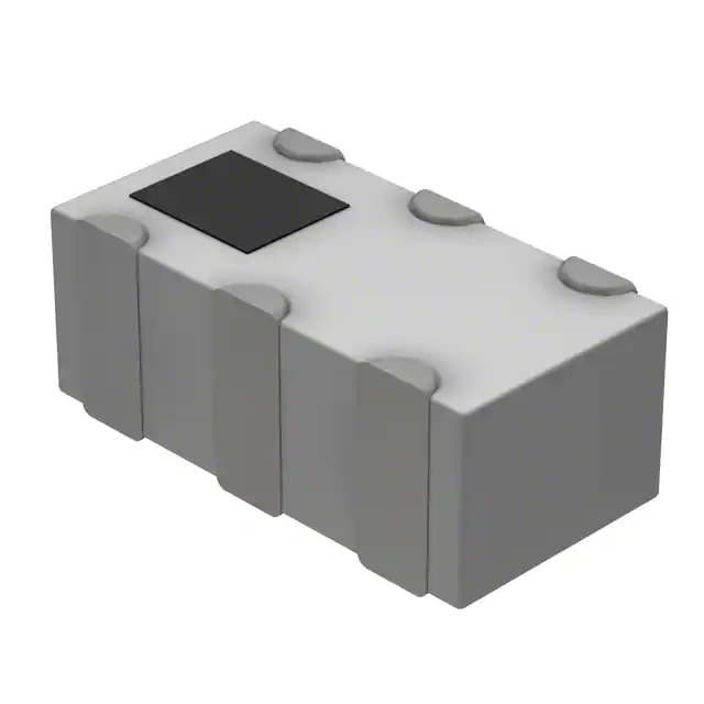
Package: CSPG (Chip Scale Package Glass), 8-bump flip-chip, 2.15 mm × 1.85 mm footprint, 0.63 mm nominal height, ECOPACK2-compliant.
| Pin/Terminal | Circuit Role | Design Meaning |
|---|---|---|
| A1 | Tx filter input | Connects directly to STM32WL RFO_HP pin; accepts high-power Tx signal before harmonic filtering |
| A2 | Differential-N Rx balun output | One leg of balanced output from STM32WL RFI_N_out; requires controlled 64 Ω differential trace |
| A3 | Differential-P Rx balun output | Other leg of balanced output from STM32WL RFI_P_out; paired with A2 for impedance-controlled routing |
| B1, B2, C2 | Ground terminals | Three dedicated GND bumps (GND1–GND3) for low-inductance RF return path and thermal dissipation |
| C1 | Tx filter output | 50 Ω single-ended output to antenna; designed for direct connection to 50 Ω RF trace or matching network |
| C3 | Rx balun input | Single-ended input from antenna; feeds internal balun to generate differential RFI_P/N signals for MCU |
Key Features
| Feature | Design Value |
|---|---|
| Integrated balun + Tx harmonic filter | Eliminates need for discrete matching components and external harmonic filters, reducing RF BOM count by ≥4 parts |
| STM32WL-optimized impedance matching | Conjugate match to RFI_P/N_out (64 Ω diff) and RFO_HP (53 Ω), enabling plug-and-play integration without tuning |
| Deep harmonic suppression | ≥45 dB rejection at 2f₀ and ≥21 dB at 10f₀ - meets regulatory spectral purity requirements for LPWAN deployments |
| Ultra-miniature CSPG package | 2.15 mm × 1.85 mm footprint with 0.63 mm max height - supports compact module designs for wearables and sensor nodes |
| IPD-on-glass technology | Enables stable RF performance across temperature (-40 to +105 °C) and superior Q-factor vs. LTCC or laminate-based baluns |
Applications
| Smart Utility Metering | Industrial Sensor Networks |
|---|---|
|
Use Scenario: Battery-powered gas/water meters transmitting daily consumption data over 5–10 km using LoRa® in 470–510 MHz ISM band. IC Role / Device Role / Timing Role: RF front-end balun and harmonic filter interfacing STM32WL RFO_HP and RFI_P/N_out to monopole antenna. Use Value: Enables certified Class A LoRaWAN operation with >15-year battery life by minimizing Tx insertion loss and eliminating external filter components. |
Use Scenario: Wireless vibration/temperature sensors deployed in factory machinery, reporting condition data via (G)FSK every 5 minutes. IC Role / Device Role / Timing Role: Single-chip RF interface providing matched 50 Ω antenna port and differential Rx conversion for STM32WL baseband processing. Use Value: Reduces PCB area by 3.2 mm² vs. discrete balun+filter solution while maintaining >19 dB Rx return loss across operating temperature range. |
| Asset Tracking Tags | Smart Agriculture Nodes |
|
Use Scenario: GPS-less logistics tags using geolocation via multi-hop LoRa® mesh in rural areas with limited gateway density. IC Role / Device Role / Timing Role: Harmonic-filtering balun ensuring clean spectral emission during high-power (14 dBm) burst transmissions. Use Value: Achieves FCC Part 15.247 compliance without post-PCB tuning, accelerating time-to-certification by ≥3 weeks. |
Use Scenario: Solar-powered soil moisture sensors transmitting BPSK-modulated data twice daily from remote fields. IC Role / Device Role / Timing Role: Low-profile RF interface enabling 630 μm total stack height for conformal enclosure sealing and IP68 rating. Use Value: Maintains <±0.3 dB amplitude imbalance across -40 to +85 °C, preserving Rx sensitivity stability in outdoor thermal cycling. |
Equivalent & Alternatives
The following parts are listed as comparable options for similar RF front-end balun + filter applications.
| Alternative Part | Technical Difference | Application Difference | Selection Advice |
|---|---|---|---|
| TDK MM8201-2705 | Discrete 3-component solution (balun + two LC filters); 3.2 mm × 2.5 mm 0402-footprint area; no integrated harmonics filter beyond 3f₀ | Requires manual impedance tuning for STM32WL; supports wider 433–527 MHz band but lacks 470–510 MHz optimization | Select when board-level tuning capability exists and cost-per-unit is prioritized over design cycle time |
| Qorvo QPFM1001 | Monolithic GaAs balun+filter; 2.0 mm × 1.6 mm; 4.2 dB higher Tx insertion loss (6.35 dB typ); 32 dB 2f₀ rejection | Validated for Semtech SX126x, not STM32WL; requires external DC blocking caps and matching network | Select only for cross-platform designs where Qorvo's ecosystem tooling offsets STM32WL-specific optimization loss |
Compared with TDMM8201-2705 and QPFM1001, BALFLB-WL-07D3 delivers lowest system-level RF BOM count, highest harmonic rejection in the 470–510 MHz band, and guaranteed impedance match to STM32WL's native pinout - reducing layout risk and eliminating post-layout tuning.
Availability
BALFLB-WL-07D3 is available at Aetrix Electronics and suitable for smart utility metering, industrial sensor networks, asset tracking tags, and smart agriculture nodes requiring stable component supply, full ECOPACK2 compliance, and validated RF performance for STM32WL-based LPWAN designs.
Supply support for BALFLB-WL-07D3 includes scheduled delivery planning, volume procurement assistance, BOM continuity management, traceable sourcing, and lifecycle availability coordination for OEM customers, industrial embedded developers, connected-device designers, and electronics production programs.
Manufacturer
STMicroelectronics is a global semiconductor leader headquartered in Geneva, Switzerland, designing and manufacturing microcontrollers, analog ICs, MEMS, and power devices for industrial, automotive, and IoT markets.
BALFLB-WL-07D3 belongs to ST's IPD (Integrated Passive Device) RF portfolio, engineered specifically to simplify RF front-end design for its STM32WL wireless MCUs - reducing time-to-market for certified sub-GHz LPWAN endpoints.
FAQ
Is BALFLB-WL-07D3 compatible with STM32WL55JC and STM32WL54JC variants?
Yes - BALFLB-WL-07D3 is qualified for all BGA-packaged STM32WL microcontrollers, including WL54 and WL55 variants. Its impedance matching targets the RFO_HP and RFI_P/N_out pins common across the family, and its 470–510 MHz performance aligns with the sub-GHz transceiver's high-power mode specification in those devices.
What is the recommended PCB stack-up for optimal RF performance?
The validated stack-up uses a 4-layer board with 80–140 µm dielectric thickness between layer 1 (signal) and layer 2 (solid ground plane). Critical RF traces - RFO_out (50 Ω), RFI_in (50 Ω), RFO_HP (53 Ω), and RFI_out differential pair (Zodd = 53 Ω) - must follow exact width/spacing per DS14108 Table 7 to maintain target impedances.
Does BALFLB-WL-07D3 require external DC blocking capacitors?
No - the device is internally DC-coupled on all RF paths. The RFO_in, RFO_out, RFI_in, RFI_P_out, and RFI_N_out terminals are designed for direct connection to STM32WL pins and antenna without series capacitors, simplifying layout and preserving low-frequency response for FSK/BPSK modulation.
Can BALFLB-WL-07D3 be used outside the 470–510 MHz band?
Performance is not characterized or guaranteed outside 470–510 MHz. While basic functionality may occur at adjacent frequencies (e.g., 433 MHz or 868 MHz), Rx imbalance, Tx harmonic rejection, and return loss degrade significantly - ST specifies no operating parameters beyond this band, and regulatory compliance cannot be assumed.
BALFLB-WL-07D3 Specifications
- Product attributes
- Attribute value
- Manufacturer:
- STMicroelectronics
- Series:
- -
- Package/Case:
- 8-WFBGA, CSPBGA
- Packaging:
- Tape & Reel (TR)
- Product Status:
- Active
- Frequency Range:
- 470MHz ~ 510MHz
- Impedance - Unbalanced/Balanced:
- -
- Phase Difference:
- 0°
- Insertion Loss (Max):
- 2.05dB
- Return Loss (Min):
- 16dB
- Mounting Type:
- Surface Mount
BALFLB-WL-07D3 FAQ
1.How can I place an order for BALFLB-WL-07D3 through Aetrix?
Please submit a Request for Quotation (RFQ) for BALFLB-WL-07D3 on Aetrix. Our sales agent will provide a competitive quotation and guide you through the order confirmation once you accept the terms.
2.Are the price and stock information for BALFLB-WL-07D3 reliable?
The price and inventory of BALFLB-WL-07D3 are updated periodically and may fluctuate due to market conditions. Stock and pricing data are typically refreshed every 24 hours. Quotation validity for BALFLB-WL-07D3 is usually 5 days.
3.What payment methods are accepted for BALFLB-WL-07D3?
We accept Wire Transfer, PayPal, Credit Card, Western Union, MoneyGram, and Escrow for BALFLB-WL-07D3 transactions.
Note: Certain payment methods may incur a processing fee.
4.How is shipping managed for BALFLB-WL-07D3?
BALFLB-WL-07D3 orders can be shipped via leading logistics carriers, including DHL, UPS, FedEx, TNT, or Registered Mail.
Once your BALFLB-WL-07D3 order is processed, you will receive an email with the shipment details and tracking number.
Note: Tracking information may take up to 24 hours to appear. Express delivery typically takes 3–5 business days.
5.How can I obtain technical support or documentation for BALFLB-WL-07D3?
For technical support, including BALFLB-WL-07D3 datasheets, pinout diagrams, or application guidance, please contact our engineering support team. They can provide detailed documentation and assistance for your BALFLB-WL-07D3 requirements.
6.How does Aetrix verify that BALFLB-WL-07D3 is sourced from the original manufacturer or authorized distributors?
All BALFLB-WL-07D3 products on Aetrix are procured from qualified distributors and authorized channels. Our dedicated quality assurance team conducts strict verification, including traceability checks and, if necessary, third-party testing. This ensures that BALFLB-WL-07D3 meets industry standards.
7.What is the process for return or replacement of BALFLB-WL-07D3?
All BALFLB-WL-07D3 units undergo pre-shipment inspection (PSI). If there is an issue with BALFLB-WL-07D3, returns or replacements are accepted under the following conditions:
1.Quantity discrepancies, incorrect items, or visible external defects (such as breakage or corrosion), acknowledged by Aetrix.
2.The issue is reported within 90 days of delivery.
3.The BALFLB-WL-07D3 part is unused and in its original packaging.
Return procedure for BALFLB-WL-07D3:
1.Submit a request within 90 days.
2.Obtain a Return Material Authorization (RMA) from Aetrix.
BALFLB-WL-07D3 Tags

-
2450BL15B0100001E
Johanson Technology Inc.
-
0900BL15D0050001E
Johanson Technology Inc.
-
0900PC16J0042001E
Johanson Technology Inc.
-
2450BM15A0002001E
Johanson Technology Inc.
-
2450BM14G0011001T
Johanson Technology Inc.
-
BD0810N50100AHF
TTM Technologies, Inc.
-
1720BL15B0050001E
Johanson Technology Inc.
-
0900PC15A0036001E
Johanson Technology Inc.
-
0868BM15C0001001E
Johanson Technology Inc.
-
0915BM15A0001001E
Johanson Technology Inc.
-
HHM1776B3
TDK Corporation
-
2450BM14E0003001T
Johanson Technology Inc.
Tech Hub

A practical engineering and sourcing framework covering lifecycle verification, lifetime-buy calculations, replacement qualification, supplier checks and counterfeit-risk controls.

TTL and CMOS logic families differ in thresholds, loading, output drive, power and timing. This engineering guide compares 74HC and 74HCT, calculates noise margins and checks 3.3 V/5 V compatibility.

A practical engineering guide to 3.3V and 5V logic compatibility, input thresholds, resistor dividers, translator ICs, MOSFET level shifting, I2C pull-ups, timing limits and power-sequencing risks.

The 74HC595 uses push-pull logic outputs, while the TPIC6B595 uses 50 V open-drain DMOS sinks for higher-power loads. This guide compares timing, current limits, 3.3 V interfacing, load wiring, thermal…

The 74HC595 converts serial data into eight stable parallel outputs. This guide covers pin functions, shift and storage timing, OE and MR behavior, drive-current limits, cascading, voltage compatibilit…

A technical comparison of level-sensitive latches and edge-triggered flip-flops, covering timing windows, setup and hold limits, master–slave operation, time borrowing, race-through, HDL inference and…

A D latch stores one bit while Enable controls when data can pass. This reference covers gate-level operation, truth tables, transparency, setup and hold timing, LE versus OE, common ICs and practical …

An SR latch stores one bit through cross-coupled feedback. This engineering reference covers NOR and NAND implementations, truth tables, forbidden-state recovery, gated operation, switch debouncing, fa…

Latch circuits retain one bit through feedback. This technical reference covers SR and D latches, truth tables, transparency, timing limits, latch-versus-flip-flop behavior, applications and common log…

An engineering guide to LED driver operation, constant-current and constant-voltage outputs, linear and switching topologies, dimming, IC selection, calculations, replacement compatibility, and fault c…


