
 My Inquiry
 My Account


STMicroelectronics BALF-NRF01E3
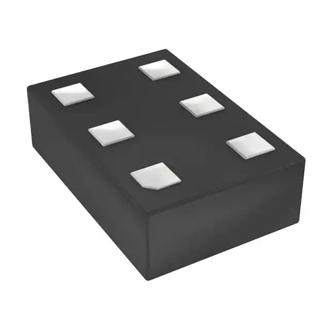
- Part No.:
- BALF-NRF01E3
- Manufacturer:
- STMicroelectronics
- Category:
- Balun
- Package:
- 6-XFLGA
- Datasheet:
-
 BALF-NRF01E3.pdf
- Description:
- BALUN 2.4GHZ-2.54GHZ 6XFLGA
- Quantity:
- Payment:

- Shipping:

Inventory:51,101
Please send an inquiry. Send us your inquiry, and we will respond immediately.
Product details
Overview
BALF-NRF01E3 from STMicroelectronics is an ultraminiature 2.45 GHz balun with integrated matching network and harmonic filtering, designed for differential RF interface between Nordic nRF51822-QFAA/AB/AC and nRF51422-QFAA/AB/AC transceivers and antenna. It provides 50 Ω single-ended input, conjugate-matched differential output, 2.2–2.7 dB insertion loss, <1 dB amplitude imbalance, and ±10° phase imbalance across 2400–2540 MHz.
For engineers reviewing the BALF-NRF01E3 datasheet, BALF-NRF01E3 pinout, BALF-NRF01E3 application, or BALF-NRF01E3 equivalent, key selection criteria include its LGA-6 package footprint (<1.5 mm²), ESD robustness (2000 V HBM), -40°C to +105°C operating range, and optimized impedance match for Nordic BLE SoCs in space-constrained IoT endpoints.
Technical Context
The BALF-NRF01E3 implements a monolithic IPD (Integrated Passive Device) balun on non-conductive glass substrate, enabling high Q-factor and low parasitic coupling. Its internal matching network is fixed and pre-tuned to deliver conjugate match specifically to the RF ports of nRF51822/nRF51422 chipsets-eliminating external discrete matching components.
It integrates a 2nd-harmonic filter (15.8–16.3 dB rejection at 4800–5080 MHz) and 3rd-harmonic filter (22.7–24.1 dB rejection at 7200–7620 MHz), supporting regulatory compliance for spurious emissions. The device operates passively with no bias required beyond VCC (used only for ESD protection path).
Key Specifications
| Parameter | Value and Actual Design Meaning |
|---|---|
| Frequency Range | 2400–2540 MHz bandwidth covering full 2.4 GHz ISM band for BLE operation |
| Insertion Loss | 2.2–2.7 dB typical - directly impacts RF link budget and transmit efficiency |
| Amplitude Imbalance | −1 to +0.3 dB - ensures balanced I/Q signal integrity for modulation fidelity |
| Phase Imbalance | −10° to +10° - maintains orthogonality critical for differential receiver sensitivity |
| Return Loss | 14–15 dB minimum - indicates >96% power transfer at SE port under matched conditions |
| ESD Rating (HBM) | 2000 V - enables robust handling during PCB assembly and field deployment |
| Operating Temp | −40°C to +105°C - supports industrial-grade BLE node operation without derating |
Pinout & Package
LGA-6 package (1.5 × 1.0 × 0.45 mm), epoxy UL94-V0 compliant, lead-free, exposed pad not electrically connected. Glass-based IPD construction enables stable RF performance across temperature and humidity.
| Pin/Terminal | Circuit Role | Design Meaning |
|---|---|---|
| 1 ANT | Single-ended RF input | Connects to transceiver's RFIO pin; 50 Ω nominal impedance interface |
| 2 GND | Ground reference | RF and DC return path; must be low-inductance connection to solid ground plane |
| 3 BAL− | Differential RF output (negative) | Drives negative leg of differential antenna feed or balun-coupled PA/LNA |
| 4 BAL+ | Differential RF output (positive) | Drives positive leg; paired with BAL− to form 100 Ω differential output |
| 5 VCC | ESD protection supply | No active biasing; connects to local 3.3 V rail solely for ESD clamp functionality |
| 6 NC | No connect | Internally unconnected; must remain floating per design |
Key Features
| Feature | Design Value |
|---|---|
| Monolithic IPD on glass | Enables <1.5 mm² footprint and eliminates discrete matching component count |
| Pre-tuned conjugate match | Optimized ZOUT for nRF51822/nRF51422 RF ports - no external tuning required |
| Integrated 2nd/3rd harmonic filtering | Provides ≥15.8 dB suppression at 4.8–5.1 GHz and ≥22.7 dB at 7.2–7.6 GHz |
| LGA-6 land grid array | Compatible with standard SMT reflow; 0.2 mm pitch, 0.4 mm height for ultra-low profile integration |
Applications
| BLE Wearable Sensor Node | Smart Home Hub Transceiver |
|---|---|
Use Scenario: Compact wrist-worn BLE sensor transmitting heart rate and motion data at 2.4 GHz. IC Role / Device Role / Timing Role: Balun and harmonic filter between nRF51422-QFAA and PCB trace antenna. Use Value: Reduces BOM by eliminating 4–6 discrete matching components while maintaining >96% RF power transfer efficiency. | Use Scenario: Battery-powered smart thermostat relaying environmental data via BLE mesh. IC Role / Device Role / Timing Role: Single-ended to differential RF interface with integrated harmonic suppression for FCC/CE compliance. Use Value: Achieves 22.7+ dB 3rd-harmonic rejection without external filters, simplifying layout and passing conducted emission tests. |
| Medical Patch Monitor | Industrial Asset Tag |
Use Scenario: Disposable skin-adhesive patch monitoring ECG and temperature over 7-day wear cycle. IC Role / Device Role / Timing Role: Miniaturized RF front-end balun enabling sub-10 mm² total RF section area. Use Value: Enables 1.5 mm² footprint and 0.45 mm height - critical for conformal, low-profile medical packaging. | Use Scenario: Ruggedized metal-tagged BLE beacon tracking warehouse pallets in −25°C to +70°C environments. IC Role / Device Role / Timing Role: Temperature-stable balun interfacing nRF51822-QFAC to ceramic chip antenna. Use Value: Maintains <1 dB amplitude imbalance across −40°C to +105°C - preserves BLE packet error rate under thermal stress. |
Equivalent & Alternatives
The following parts are listed as comparable options for similar balun-with-filter applications.
| Alternative Part | Technical Difference | Application Difference | Selection Advice |
|---|---|---|---|
| SKY13370-374LF | Higher IL (3.0 dB typ), wider bandwidth (2.4–2.5 GHz), no integrated harmonic filtering | Requires external LC filter for harmonics; larger 1.6 × 1.2 mm package | Select when broader frequency margin needed but harmonic filtering handled separately |
| DA221ZM10 | 0.6 dB higher IL (3.3 dB typ), no VCC pin, 2-pin configuration (no dedicated GND) | Lacks ESD protection path; unsuitable for high-handling-volume manufacturing | Choose only for cost-sensitive, low-reliability consumer prototypes with simplified layout |
Compared with SKY13370-374LF and DA221ZM10, BALF-NRF01E3 delivers lower insertion loss, built-in harmonic filtering, and ESD-protected VCC-making it optimal for production-grade BLE devices where size, regulatory compliance, and assembly yield are critical.
Availability
BALF-NRF01E3 is available at Aetrix Electronics and suitable for BLE wearable sensors, smart home hubs, medical patches, and industrial asset tags requiring stable component supply and guaranteed long-term availability.
Supply support for BALF-NRF01E3 includes scheduled delivery planning, volume procurement assistance, BOM continuity management, traceable sourcing, and lifecycle availability coordination for OEM customers, industrial embedded developers, connected-device designers, and electronics production programs.
Manufacturer
STMicroelectronics is a global semiconductor leader headquartered in Geneva, delivering silicon solutions for automotive, industrial, and personal electronics markets since 1987.
BALF-NRF01E3 belongs to ST's IPAD™ family of integrated passive devices, engineered specifically for miniaturized 2.4 GHz wireless front-ends in battery-powered IoT nodes.
FAQ
Is BALF-NRF01E3 compatible with nRF52832 or nRF52840 series?
No. BALF-NRF01E3 is specifically tuned for nRF51822 and nRF51422 RF ports. Its conjugate match network does not align with the 52-series impedance profiles, resulting in >3 dB additional insertion loss and degraded return loss. ST recommends BALF-NRF02D3 for nRF52832 compatibility.
Can VCC pin be left unconnected?
No. VCC must be connected to the same 3.3 V supply used by the nRF51 SoC. Though not a power rail, it enables the internal ESD protection diode clamping path. Leaving it floating degrades HBM rating from 2000 V to <500 V and risks latch-up during ESD events.
What is the recommended PCB stack-up for optimal RF performance?
A 4-layer stack-up with dedicated inner ground plane adjacent to the top layer (where BALF-NRF01E3 is placed) is required. Antenna trace must be on Layer 1, with continuous ground reference on Layer 2 and no splits or vias within 3 mm of the balun pads. Use 0.2 mm solder mask defined pads per Figure 16.
Does BALF-NRF01E3 require external DC blocking capacitors?
No. The device is fully AC-coupled internally. No external DC blocking capacitors are needed on BAL+ or BAL− outputs. Adding them introduces parasitic inductance that degrades amplitude/phase balance above 2.4 GHz and violates the validated reference layout in Figure 8.
BALF-NRF01E3 Specifications
- Product attributes
- Attribute value
- Manufacturer:
- STMicroelectronics
- Series:
- -
- Package/Case:
- 6-XFLGA
- Packaging:
- Tape & Reel (TR)
- Product Status:
- Active
- Frequency Range:
- 2.4GHz ~ 2.54GHz
- Impedance - Unbalanced/Balanced:
- 50 / -Ohm
- Phase Difference:
- 4°
- Insertion Loss (Max):
- 2.2dB
- Return Loss (Min):
- 15dB
- Mounting Type:
- Surface Mount
BALF-NRF01E3 FAQ
1.How can I place an order for BALF-NRF01E3 through Aetrix?
Please submit a Request for Quotation (RFQ) for BALF-NRF01E3 on Aetrix. Our sales agent will provide a competitive quotation and guide you through the order confirmation once you accept the terms.
2.Are the price and stock information for BALF-NRF01E3 reliable?
The price and inventory of BALF-NRF01E3 are updated periodically and may fluctuate due to market conditions. Stock and pricing data are typically refreshed every 24 hours. Quotation validity for BALF-NRF01E3 is usually 5 days.
3.What payment methods are accepted for BALF-NRF01E3?
We accept Wire Transfer, PayPal, Credit Card, Western Union, MoneyGram, and Escrow for BALF-NRF01E3 transactions.
Note: Certain payment methods may incur a processing fee.
4.How is shipping managed for BALF-NRF01E3?
BALF-NRF01E3 orders can be shipped via leading logistics carriers, including DHL, UPS, FedEx, TNT, or Registered Mail.
Once your BALF-NRF01E3 order is processed, you will receive an email with the shipment details and tracking number.
Note: Tracking information may take up to 24 hours to appear. Express delivery typically takes 3–5 business days.
5.How can I obtain technical support or documentation for BALF-NRF01E3?
For technical support, including BALF-NRF01E3 datasheets, pinout diagrams, or application guidance, please contact our engineering support team. They can provide detailed documentation and assistance for your BALF-NRF01E3 requirements.
6.How does Aetrix verify that BALF-NRF01E3 is sourced from the original manufacturer or authorized distributors?
All BALF-NRF01E3 products on Aetrix are procured from qualified distributors and authorized channels. Our dedicated quality assurance team conducts strict verification, including traceability checks and, if necessary, third-party testing. This ensures that BALF-NRF01E3 meets industry standards.
7.What is the process for return or replacement of BALF-NRF01E3?
All BALF-NRF01E3 units undergo pre-shipment inspection (PSI). If there is an issue with BALF-NRF01E3, returns or replacements are accepted under the following conditions:
1.Quantity discrepancies, incorrect items, or visible external defects (such as breakage or corrosion), acknowledged by Aetrix.
2.The issue is reported within 90 days of delivery.
3.The BALF-NRF01E3 part is unused and in its original packaging.
Return procedure for BALF-NRF01E3:
1.Submit a request within 90 days.
2.Obtain a Return Material Authorization (RMA) from Aetrix.
BALF-NRF01E3 Tags

-
2450BL15B0100001E
Johanson Technology Inc.
-
0900BL15D0050001E
Johanson Technology Inc.
-
0900PC16J0042001E
Johanson Technology Inc.
-
2450BM15A0002001E
Johanson Technology Inc.
-
2450BM14G0011001T
Johanson Technology Inc.
-
BD0810N50100AHF
TTM Technologies, Inc.
-
1720BL15B0050001E
Johanson Technology Inc.
-
0900PC15A0036001E
Johanson Technology Inc.
-
0868BM15C0001001E
Johanson Technology Inc.
-
0915BM15A0001001E
Johanson Technology Inc.
-
HHM1776B3
TDK Corporation
-
2450BM14E0003001T
Johanson Technology Inc.
Tech Hub

A practical engineering and sourcing framework covering lifecycle verification, lifetime-buy calculations, replacement qualification, supplier checks and counterfeit-risk controls.

TTL and CMOS logic families differ in thresholds, loading, output drive, power and timing. This engineering guide compares 74HC and 74HCT, calculates noise margins and checks 3.3 V/5 V compatibility.

A practical engineering guide to 3.3V and 5V logic compatibility, input thresholds, resistor dividers, translator ICs, MOSFET level shifting, I2C pull-ups, timing limits and power-sequencing risks.

The 74HC595 uses push-pull logic outputs, while the TPIC6B595 uses 50 V open-drain DMOS sinks for higher-power loads. This guide compares timing, current limits, 3.3 V interfacing, load wiring, thermal…

The 74HC595 converts serial data into eight stable parallel outputs. This guide covers pin functions, shift and storage timing, OE and MR behavior, drive-current limits, cascading, voltage compatibilit…

A technical comparison of level-sensitive latches and edge-triggered flip-flops, covering timing windows, setup and hold limits, master–slave operation, time borrowing, race-through, HDL inference and…

A D latch stores one bit while Enable controls when data can pass. This reference covers gate-level operation, truth tables, transparency, setup and hold timing, LE versus OE, common ICs and practical …

An SR latch stores one bit through cross-coupled feedback. This engineering reference covers NOR and NAND implementations, truth tables, forbidden-state recovery, gated operation, switch debouncing, fa…

Latch circuits retain one bit through feedback. This technical reference covers SR and D latches, truth tables, transparency, timing limits, latch-versus-flip-flop behavior, applications and common log…

An engineering guide to LED driver operation, constant-current and constant-voltage outputs, linear and switching topologies, dimming, IC selection, calculations, replacement compatibility, and fault c…


