
 My Inquiry
 My Account


STMicroelectronics BAL-UWB-01E3
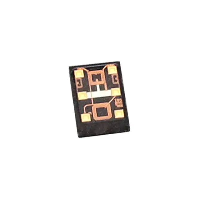
- Part No.:
- BAL-UWB-01E3
- Manufacturer:
- STMicroelectronics
- Category:
- Balun
- Package:
- 6-SMD, No Lead
- Datasheet:
-
 BAL-UWB-01E3.pdf
- Description:
- BALUN FOR UWB 3HGZ TO 8GHZ
- Quantity:
- Payment:

- Shipping:

Inventory:23,815
Please send an inquiry. Send us your inquiry, and we will respond immediately.
Product details
Overview
BAL-UWB-01E3 from STMicroelectronics is an ultra-miniature 50 Ω to 100 Ω balun IC for ultra-wideband (UWB) RF front-ends operating from 3 GHz to 8 GHz, integrating a matching network on non-conductive glass substrate using IPD technology; it delivers 1.2 dB typical insertion loss, ±2.5 dB amplitude imbalance, and ±25° phase imbalance for secure UWB ranging in vehicle keyless entry systems.
For engineers reviewing the BAL-UWB-01E3 datasheet, BAL-UWB-01E3 pinout, BAL-UWB-01E3 application, or BAL-UWB-01E3 equivalent, this page provides verified RF performance data, bumpless CSP package dimensions, differential impedance mapping, and PCB assembly guidance aligned with DS12796 Rev 2.
Technical Context
This balun converts single-ended 50 Ω RF input to balanced 100 Ω differential output using ST's integrated passive device (IPD) process on glass, enabling high isolation and minimal parasitic coupling across 3–8 GHz. Its design eliminates discrete matching components while maintaining <450 µm total thickness.
The device operates over –40 °C to +105 °C, supports 10 dBm maximum input power, and meets 2 kV HBM ESD rating-critical for robust integration into portable UWB transceivers where board space and RF integrity are constrained.
Key Specifications
| Parameter | Value and Actual Design Meaning |
|---|---|
| Frequency Range | 3 GHz to 8 GHz - full UWB channel support per IEEE 802.15.4z |
| Insertion Loss | 1.2 dB typ - ensures minimal signal attenuation in time-of-flight ranging paths |
| Amplitude Imbalance | ±2.5 dB max - maintains accurate differential signaling for precise phase-based distance calculation |
| Phase Imbalance | ±25° max - preserves waveform symmetry critical for sub-centimeter UWB ranging accuracy |
| Differential Impedance | 100 Ω nominal - matches standard UWB transceiver differential I/O interfaces |
| Single-Ended Impedance | 50 Ω nominal - directly interfaces with antenna feedlines without external matching |
| ESD Rating | 2000 V HBM - protects against handling-induced discharge during SMT assembly |
Pinout & Package
Bumpless CSP (Chip-Scale Package) with 6 solderable pads on non-conductive glass substrate; total thickness ≤ 425 µm; footprint compatible with LGA reflow processes; no bumps-direct copper pad contact.
| Pin/Terminal | Circuit Role | Design Meaning |
|---|---|---|
| SE | Single-ended RF input | Connects directly to UWB transceiver SE output or antenna feedline at 50 Ω |
| DIFFp | Differential positive output | Drives positive leg of differential UWB receiver/transmitter path |
| DIFFn | Differential negative output | Drives negative leg; paired with DIFFp to form 100 Ω balanced interface |
| GND1, GND2 | RF ground terminals | Provide low-inductance return paths; must be connected to solid RF ground plane |
| NC | No-connect pad | Not internally bonded; left unconnected per design-no routing or stitching required |
Key Features
| Feature | Design Value |
|---|---|
| Ultra-low profile (≤ 425 µm) | Enables integration into slim wearable and tag form factors without height compromise |
| Integrated matching network | Eliminates ≥3 external RF components, reducing BOM count and layout area by >2 mm² |
| IPD-on-glass construction | Delivers stable Q-factor and low dielectric loss across full UWB band vs. silicon-based alternatives |
| LGA-compatible footprint | Supports standard reflow profiles and automated optical inspection without bump-related defects |
Applications
| High-Value Asset Tracking | Vehicle Keyless Entry |
|---|---|
Use Scenario: Real-time location of pallets, tools, or medical equipment indoors using UWB time-difference-of-arrival (TDOA). IC Role / Device Role / Timing Role: Balun interface between UWB SoC and patch antenna, preserving signal fidelity for <10 cm ranging accuracy. Use Value: Enables sub-15 cm precision at 10 Hz update rate with 1.2 dB insertion loss minimizing SNR degradation. | Use Scenario: Secure hands-free vehicle access via UWB-based secure ranging and authentication. IC Role / Device Role / Timing Role: Differential RF interface for UWB transceiver in fob or smartphone, supporting IEEE 802.15.4z PHY layer. Use Value: ±2.5 dB amplitude and ±25° phase imbalance ensure reliable angle-of-arrival (AoA) estimation for anti-relay protection. |
| Healthcare Patient Monitoring | Secure Entry / Transaction |
Use Scenario: Contactless fall detection and proximity monitoring in assisted-living facilities using UWB wall-mounted anchors. IC Role / Device Role / Timing Role: Balun converting SoC SE output to balanced antenna feed for low-jitter impulse radio transmission. Use Value: 3–8 GHz bandwidth coverage enables multi-channel hopping to mitigate multipath in cluttered clinical environments. | Use Scenario: Tap-to-pay or door unlock with cryptographic challenge-response using UWB secure channel. IC Role / Device Role / Timing Role: RF interface ensuring deterministic group delay and minimal jitter for time-critical secure ranging handshake. Use Value: 2000 V HBM ESD rating prevents field failure during frequent human-handling in consumer-facing devices. |
Equivalent & Alternatives
The following parts are listed as comparable options for similar UWB balun applications.
| Alternative Part | Technical Difference | Application Difference | Selection Advice |
|---|---|---|---|
| Qorvo QPB9370 | 50 Ω to 100 Ω, 6.0–10.0 GHz range, 1.5 dB IL, larger 1.6 × 1.2 mm CSP | Extends upper frequency beyond 8 GHz but lacks 3–6 GHz coverage needed for FCC UWB Channel 5 | Select only if system requires >8 GHz operation and can accommodate 30% larger PCB footprint |
| Skyworks SKY66420-31 | 50 Ω to 100 Ω, 3.1–6.5 GHz, 1.4 dB IL, 0.8 × 0.8 mm DFN | Narrower bandwidth excludes 6.5–8.0 GHz channels used in high-precision AoA and TDOA | Acceptable for cost-sensitive designs targeting only lower UWB bands, but not IEEE 802.15.4z full-band compliance |
Compared with QPB9370 and SKY66420-31, BAL-UWB-01E3 uniquely covers the full 3–8 GHz UWB spectrum in a 1.25 × 1.8 mm bumpless CSP, delivering lowest insertion loss and smallest height for space-constrained secure ranging applications.
Availability
BAL-UWB-01E3 is available at Aetrix Electronics and suitable for high-value asset tracking, vehicle keyless entry, and secure transaction systems requiring stable component supply, consistent RF performance, and long-term UWB protocol compliance.
Supply support for BAL-UWB-01E3 includes scheduled delivery planning, volume procurement assistance, BOM continuity management, traceable sourcing, and lifecycle availability coordination for OEM customers, industrial embedded developers, connected-device designers, and electronics production programs.
Manufacturer
STMicroelectronics is a global semiconductor leader headquartered in Geneva, designing and manufacturing microcontrollers, analog ICs, MEMS, and RF components for industrial, automotive, and consumer markets.
BAL-UWB-01E3 belongs to ST's UWB RF front-end portfolio, engineered specifically to enable precise, secure, and energy-efficient short-range wireless ranging in next-generation IoT and automotive access systems.
FAQ
What is the recommended PCB stack-up for optimal BAL-UWB-01E3 RF performance?
ST recommends a 4-layer stack-up with dedicated internal RF ground plane adjacent to the top layer, 0.2 mm prepreg between top signal and ground layers, and controlled-impedance 50 Ω microstrip routing from SE pad to antenna. Ground vias must surround the balun within 0.5 mm to minimize loop inductance.
Can BAL-UWB-01E3 be used with UWB transceivers other than ST's own?
Yes-BAL-UWB-01E3 is vendor-agnostic and compatible with all major UWB transceivers (e.g., Decawave DW3000, NXP SR040, Qorvo QPG6100) that require 50 Ω SE to 100 Ω differential conversion across 3–8 GHz, provided matching PCB layout rules are followed.
Is thermal relief required under the GND1 and GND2 pads during reflow?
No-thermal relief is not recommended. GND1 and GND2 must connect directly to a solid, unbroken RF ground plane with ≥8 thermal vias (0.25 mm diameter, 0.5 mm pitch) per pad to maintain low-impedance return paths and prevent RF resonance at 6 GHz.
Does the NC pad require solder mask opening or stencil aperture?
No-the NC pad must remain unconnected and uncovered by solder paste. ST specifies zero stencil aperture for the NC pad (B1); including it risks solder bridging to adjacent GND2 or DIFFn, causing RF shorting or yield loss.
BAL-UWB-01E3 Specifications
- Product attributes
- Attribute value
- Manufacturer:
- STMicroelectronics
- Series:
- -
- Package/Case:
- 6-SMD, No Lead
- Packaging:
- Tape & Reel (TR)
- Product Status:
- Active
- Frequency Range:
- 3GHz ~ 8GHz
- Impedance - Unbalanced/Balanced:
- 50 / 100Ohm
- Phase Difference:
- -
- Insertion Loss (Max):
- 1.2dB
- Return Loss (Min):
- 12dB
- Mounting Type:
- Surface Mount
BAL-UWB-01E3 FAQ
1.How can I place an order for BAL-UWB-01E3 through Aetrix?
Please submit a Request for Quotation (RFQ) for BAL-UWB-01E3 on Aetrix. Our sales agent will provide a competitive quotation and guide you through the order confirmation once you accept the terms.
2.Are the price and stock information for BAL-UWB-01E3 reliable?
The price and inventory of BAL-UWB-01E3 are updated periodically and may fluctuate due to market conditions. Stock and pricing data are typically refreshed every 24 hours. Quotation validity for BAL-UWB-01E3 is usually 5 days.
3.What payment methods are accepted for BAL-UWB-01E3?
We accept Wire Transfer, PayPal, Credit Card, Western Union, MoneyGram, and Escrow for BAL-UWB-01E3 transactions.
Note: Certain payment methods may incur a processing fee.
4.How is shipping managed for BAL-UWB-01E3?
BAL-UWB-01E3 orders can be shipped via leading logistics carriers, including DHL, UPS, FedEx, TNT, or Registered Mail.
Once your BAL-UWB-01E3 order is processed, you will receive an email with the shipment details and tracking number.
Note: Tracking information may take up to 24 hours to appear. Express delivery typically takes 3–5 business days.
5.How can I obtain technical support or documentation for BAL-UWB-01E3?
For technical support, including BAL-UWB-01E3 datasheets, pinout diagrams, or application guidance, please contact our engineering support team. They can provide detailed documentation and assistance for your BAL-UWB-01E3 requirements.
6.How does Aetrix verify that BAL-UWB-01E3 is sourced from the original manufacturer or authorized distributors?
All BAL-UWB-01E3 products on Aetrix are procured from qualified distributors and authorized channels. Our dedicated quality assurance team conducts strict verification, including traceability checks and, if necessary, third-party testing. This ensures that BAL-UWB-01E3 meets industry standards.
7.What is the process for return or replacement of BAL-UWB-01E3?
All BAL-UWB-01E3 units undergo pre-shipment inspection (PSI). If there is an issue with BAL-UWB-01E3, returns or replacements are accepted under the following conditions:
1.Quantity discrepancies, incorrect items, or visible external defects (such as breakage or corrosion), acknowledged by Aetrix.
2.The issue is reported within 90 days of delivery.
3.The BAL-UWB-01E3 part is unused and in its original packaging.
Return procedure for BAL-UWB-01E3:
1.Submit a request within 90 days.
2.Obtain a Return Material Authorization (RMA) from Aetrix.
BAL-UWB-01E3 Tags

-
2450BL15B0100001E
Johanson Technology Inc.
-
0900BL15D0050001E
Johanson Technology Inc.
-
0900PC16J0042001E
Johanson Technology Inc.
-
2450BM15A0002001E
Johanson Technology Inc.
-
2450BM14G0011001T
Johanson Technology Inc.
-
BD0810N50100AHF
TTM Technologies, Inc.
-
1720BL15B0050001E
Johanson Technology Inc.
-
0900PC15A0036001E
Johanson Technology Inc.
-
0868BM15C0001001E
Johanson Technology Inc.
-
0915BM15A0001001E
Johanson Technology Inc.
-
HHM1776B3
TDK Corporation
-
2450BM14E0003001T
Johanson Technology Inc.
Tech Hub

A practical engineering guide to 3.3V and 5V logic compatibility, input thresholds, resistor dividers, translator ICs, MOSFET level shifting, I2C pull-ups, timing limits and power-sequencing risks.

The 74HC595 uses push-pull logic outputs, while the TPIC6B595 uses 50 V open-drain DMOS sinks for higher-power loads. This guide compares timing, current limits, 3.3 V interfacing, load wiring, thermal…

The 74HC595 converts serial data into eight stable parallel outputs. This guide covers pin functions, shift and storage timing, OE and MR behavior, drive-current limits, cascading, voltage compatibilit…

A technical comparison of level-sensitive latches and edge-triggered flip-flops, covering timing windows, setup and hold limits, master–slave operation, time borrowing, race-through, HDL inference and…

A D latch stores one bit while Enable controls when data can pass. This reference covers gate-level operation, truth tables, transparency, setup and hold timing, LE versus OE, common ICs and practical …

An SR latch stores one bit through cross-coupled feedback. This engineering reference covers NOR and NAND implementations, truth tables, forbidden-state recovery, gated operation, switch debouncing, fa…

Latch circuits retain one bit through feedback. This technical reference covers SR and D latches, truth tables, transparency, timing limits, latch-versus-flip-flop behavior, applications and common log…

An engineering guide to LED driver operation, constant-current and constant-voltage outputs, linear and switching topologies, dimming, IC selection, calculations, replacement compatibility, and fault c…

Operational amplifier guide covering op amp basics, feedback, ideal vs real op amps, common configurations, buffer circuits, offset, bias current, gain-bandwidth, slew rate, rail-to-rail limits and sel…

Jumper cables guide covering safe connection order, red and black clamp placement, final ground connection, cable gauge, length, clamp quality, copper vs CCA cables, jump starter comparison and battery…


