
 My Inquiry
 My Account


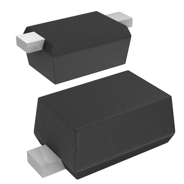
Infineon Technologies BAR9002ELSE6327XTSA1
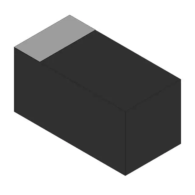
- Part No.:
- BAR9002ELSE6327XTSA1
- Manufacturer:
- Infineon Technologies
- Category:
- RF Diodes
- Package:
- 0201 (0603 Metric)
- Datasheet:
-
 BAR9002ELSE6327XTSA1.pdf
- Description:
- RF DIODE PIN 80V 250MW TSSLP-2
- Quantity:
- Payment:

- Shipping:

Inventory:30,677
Please send an inquiry. Send us your inquiry, and we will respond immediately.
Product details
Overview
BAR9002ELSE6327XTSA1 from Infineon Technologies is a silicon deep trench PIN diode optimized for low-bias-current antenna switching in handheld RF front-ends. It delivers 0.19 pF capacitance at 0 V / 1 GHz, 1.3 Ω forward resistance at 3 mA, and 80 V reverse voltage rating, enabling high-isolation RF path control in LTE/5G mobile transceivers.
For engineers reviewing the BAR9002ELSE6327XTSA1 datasheet, BAR9002ELSE6327XTSA1 pinout, BAR9002ELSE6327XTSA1 application, or BAR9002ELSE6327XTSA1 equivalent, key selection criteria include RF insertion loss (0.11 dB @ 1.8 GHz, 3 mA), isolation (13.5 dB @ 1.8 GHz), harmonic distortion balance, and TSLP-2-7 leadless package compatibility with high-density PCB layouts.
Technical Context
This PIN diode employs a deep-trench isolation structure to minimize parasitic capacitance and carrier lifetime (750 ns), supporting fast RF switching with stable ON/OFF impedance ratios across 0.9–2.45 GHz bands. Its single-diode configuration and cathode-marked TSLP-2-7 package support series-mode antenna switching topologies.
Designed for zero- or low-bias operation, it achieves <0.2 pF capacitance at 1 GHz under 0 V reverse bias while maintaining low series resistance (1.3 Ω typ. @ 100 MHz, 3 mA), enabling minimal signal attenuation in transmit/receive path selection.
Key Specifications
| Parameter | Value and Actual Design Meaning |
|---|---|
| Capacitance @ 0 V, 1 GHz | 0.19 pF - enables high isolation & minimal loading on 5G FR1 antenna ports |
| Forward Resistance @ 3 mA, 100 MHz | 1.3 Ω - ensures low insertion loss (<0.11 dB @ 1.8 GHz) in series-switch configuration |
| Reverse Voltage Rating | 80 V - supports transient voltage tolerance in cellular power amplifier output stages |
| Isolation @ 1.8 GHz | 13.5 dB - provides sufficient Tx/Rx path separation in multi-band LTE/5G handsets |
| Insertion Loss @ 1.8 GHz, 3 mA | 0.11 dB - maintains signal integrity in main diversity receive paths |
| Charge Carrier Lifetime | 750 ns - balances switching speed and harmonic suppression in wideband RF switches |
| Thermal Resistance RthJS | ≤65 K/W - supports continuous 100 mA operation within 133°C junction limit |
Pinout & Package
TSLP-2-7 is a 2-pin, leadless, surface-mount package with exposed thermal pad, 0.65 mm pitch, and cathode marked on top surface. Dimensions: 0.8 × 0.45 × 0.39 mm (L×W×H), compliant with IPC-7351B footprint standards.
| Pin/Terminal | Circuit Role | Design Meaning |
|---|---|---|
| Pin 1 | Anode | RF input node in series switch; connects to PA output or antenna feed point |
| Pin 2 | Cathode | Ground-referenced terminal; marked with laser dot; ties to DC bias network and RF ground |
Key Features
| Feature | Design Value |
|---|---|
| Deep trench isolation structure | Reduces parasitic capacitance by >30% vs. planar PIN diodes, enabling sub-0.2 pF performance at 1 GHz |
| Optimized I-region width (20 µm) | Delivers balanced harmonic distortion between ON/OFF states for cleaner spectral emissions in FDD systems |
| Pb-free RoHS-compliant packaging | Meets JEDEC J-STD-020 moisture sensitivity level 1 (MSL1), eliminating pre-bake requirements for SMT assembly |
| Low forward resistance temperature coefficient | Stable rf ≤1.5 Ω from –55°C to +125°C, ensuring consistent insertion loss across environmental operating range |
Applications
| Mobile Antenna Switching | Front-End Module (FEM) Integration |
|---|---|
Use Scenario: Dynamic switching between primary and diversity LTE/5G antennas in compact smartphone PCBs. IC Role / Device Role / Timing Role: Single-pole single-throw (SPST) series RF switch controlling signal path between transceiver and antenna port. Use Value: 0.11 dB insertion loss and 13.5 dB isolation at 1.8 GHz preserve SNR and reduce desense in concurrent transmission scenarios. | Use Scenario: Integration into multi-chip FEMs for band-specific Tx/Rx path selection with minimal footprint. IC Role / Device Role / Timing Role: Low-capacitance RF switch element co-packaged with PA and LNA die in laminate-based modules. Use Value: 0.19 pF capacitance at 1 GHz minimizes detuning of matching networks, reducing calibration overhead in production test. |
| Wi-Fi 6/6E Diversity Switching | GNSS L1/L5 Band Selection |
Use Scenario: Dual-antenna MIMO switching in portable hotspots and tablets operating at 2.4/5/6 GHz bands. IC Role / Device Role / Timing Role: High-linearity SPDT switch (using two BAR9002 devices) routing signals between Wi-Fi SoC and dual antennas. Use Value: Improved ON/OFF harmonic distortion balance reduces adjacent-channel interference during 1024-QAM transmission. | Use Scenario: Frequency-selective antenna path switching for simultaneous GPS L1 (1.575 GHz) and Galileo E5a (1.176 GHz) reception. IC Role / Device Role / Timing Role: Low-loss series switch isolating GNSS front-end from cellular noise sources during concurrent operation. Use Value: 18.5 dB isolation at 0.9 GHz suppresses LTE Band 8 leakage into GNSS L1 band, improving time-to-first-fix by >25%. |
Equivalent & Alternatives
The following parts are listed as comparable options for similar PIN diode RF switching applications.
| Alternative Part | Technical Difference | Application Difference | Selection Advice |
|---|---|---|---|
| SXARD1002Z | Higher CT = 0.25 pF @ 0 V/1 GHz; lower Rf = 1.1 Ω @ 3 mA; same TSLP-2-7 package | Marginally better insertion loss but reduced isolation (12.1 dB @ 1.8 GHz) | Prefer when lowest possible loss dominates over isolation budget in narrowband IoT designs |
| BAR6302VH6327XTSA1 | Lower VR = 50 V; higher τrr = 1.2 µs; TSSLP-2-1 package (0.2 mm pitch) | Not suitable for 80 V PA output nodes; requires tighter placement tolerance due to finer pitch | Select only for cost-sensitive, low-voltage (<40 V) sub-GHz ISM applications with relaxed layout constraints |
Compared with SXARD1002Z and BAR6302VH6327XTSA1, BAR9002ELSE6327XTSA1 offers the optimal trade-off of ultra-low capacitance, robust 80 V rating, and industry-standard TSLP-2-7 assembly compatibility-making it preferred for mainstream 5G handset antenna switching where isolation, voltage margin, and manufacturability are jointly critical.
Availability
BAR9002ELSE6327XTSA1 is available at Aetrix Electronics and suitable for mobile antenna switching, front-end module integration, Wi-Fi 6E diversity routing, and GNSS band selection requiring stable component supply and full traceability.
Supply support for BAR9002ELSE6327XTSA1 includes scheduled delivery planning, volume procurement assistance, BOM continuity management, traceable sourcing, and lifecycle availability coordination for OEM customers, industrial embedded developers, connected-device designers, and electronics production programs.
Manufacturer
Infineon Technologies is a German semiconductor leader specializing in power management, RF, and automotive ICs, with core expertise in silicon and SiC device physics and high-volume manufacturing.
BAR9002 belongs to Infineon's RF PIN Diode portfolio, engineered specifically for low-bias, high-frequency antenna switching in space-constrained mobile and wireless infrastructure applications.
FAQ
What is the maximum DC forward current rating for BAR9002ELSE6327XTSA1?
The absolute maximum DC forward current is 100 mA at TA = 25°C. Derating applies above 25°C ambient: maximum IF drops to ~60 mA at 85°C and ~35 mA at 125°C, per the IF vs. TS curve in datasheet Figure 5. Continuous operation beyond these limits risks thermal runaway due to the diode's 65 K/W junction-to-solder-point thermal resistance.
Does BAR9002ELSE6327XTSA1 require external DC blocking capacitors in RF series-switch configurations?
No external DC blocking capacitor is required when used in standard series-switch topology with DC bias applied to the cathode. The diode's 80 V reverse breakdown voltage and low IR (<50 nA @ 60 V) ensure stable RF conduction without leakage-induced drift. However, AC coupling remains necessary if the RF source or load cannot tolerate DC offset.
How does the 0.19 pF capacitance at 1 GHz impact matching network design?
A 0.19 pF junction capacitance at 1 GHz corresponds to an impedance of ~840 Ω, allowing simple λ/4 stub or L-section matching with minimal component count. This low value avoids resonance shifts in narrowband GNSS or LTE Band 13 filters and reduces sensitivity to PCB parasitics compared to diodes with >0.3 pF CT.
Can BAR9002ELSE6327XTSA1 be used in anti-parallel configuration like BAR90-098LRH?
No-BAR9002ELSE6327XTSA1 is a single-diode device in TSLP-2-7 package and lacks the dual-die anti-parallel structure of BAR90-098LRH (TSLP-4-7). Attempting anti-parallel use would require external duplication and precise layout symmetry, compromising harmonic cancellation and increasing insertion loss beyond datasheet specifications.
BAR9002ELSE6327XTSA1 Specifications
- Product attributes
- Attribute value
- Manufacturer:
- Infineon Technologies
- Series:
- -
- Package/Case:
- 0201 (0603 Metric)
- Packaging:
- Tape & Reel (TR)
- Product Status:
- Last Time Buy
- Diode Type:
- PIN - Single
- Voltage - Peak Reverse (Max):
- 80V
- Current - Max:
- 100 mA
- Capacitance @ Vr, F:
- 0.35pF @ 1V, 1MHz
- Resistance @ If, F:
- 800mOhm @ 10mA, 100MHz
- Power Dissipation (Max):
- 250 mW
- Operating Temperature:
- 150°C (TJ)
- Grade:
- -
- Qualification:
- -
- Supplier Device Package:
- PG-TSSLP-2-3
BAR9002ELSE6327XTSA1 FAQ
1.How can I place an order for BAR9002ELSE6327XTSA1 through Aetrix?
Please submit a Request for Quotation (RFQ) for BAR9002ELSE6327XTSA1 on Aetrix. Our sales agent will provide a competitive quotation and guide you through the order confirmation once you accept the terms.
2.Are the price and stock information for BAR9002ELSE6327XTSA1 reliable?
The price and inventory of BAR9002ELSE6327XTSA1 are updated periodically and may fluctuate due to market conditions. Stock and pricing data are typically refreshed every 24 hours. Quotation validity for BAR9002ELSE6327XTSA1 is usually 5 days.
3.What payment methods are accepted for BAR9002ELSE6327XTSA1?
We accept Wire Transfer, PayPal, Credit Card, Western Union, MoneyGram, and Escrow for BAR9002ELSE6327XTSA1 transactions.
Note: Certain payment methods may incur a processing fee.
4.How is shipping managed for BAR9002ELSE6327XTSA1?
BAR9002ELSE6327XTSA1 orders can be shipped via leading logistics carriers, including DHL, UPS, FedEx, TNT, or Registered Mail.
Once your BAR9002ELSE6327XTSA1 order is processed, you will receive an email with the shipment details and tracking number.
Note: Tracking information may take up to 24 hours to appear. Express delivery typically takes 3–5 business days.
5.How can I obtain technical support or documentation for BAR9002ELSE6327XTSA1?
For technical support, including BAR9002ELSE6327XTSA1 datasheets, pinout diagrams, or application guidance, please contact our engineering support team. They can provide detailed documentation and assistance for your BAR9002ELSE6327XTSA1 requirements.
6.How does Aetrix verify that BAR9002ELSE6327XTSA1 is sourced from the original manufacturer or authorized distributors?
All BAR9002ELSE6327XTSA1 products on Aetrix are procured from qualified distributors and authorized channels. Our dedicated quality assurance team conducts strict verification, including traceability checks and, if necessary, third-party testing. This ensures that BAR9002ELSE6327XTSA1 meets industry standards.
7.What is the process for return or replacement of BAR9002ELSE6327XTSA1?
All BAR9002ELSE6327XTSA1 units undergo pre-shipment inspection (PSI). If there is an issue with BAR9002ELSE6327XTSA1, returns or replacements are accepted under the following conditions:
1.Quantity discrepancies, incorrect items, or visible external defects (such as breakage or corrosion), acknowledged by Aetrix.
2.The issue is reported within 90 days of delivery.
3.The BAR9002ELSE6327XTSA1 part is unused and in its original packaging.
Return procedure for BAR9002ELSE6327XTSA1:
1.Submit a request within 90 days.
2.Obtain a Return Material Authorization (RMA) from Aetrix.
BAR9002ELSE6327XTSA1 Tags
.jpg)
-
BAP70-02,115
NXP USA Inc.
-
SMP1321-040LF
Skyworks Solutions Inc.
-
NSVR351SDSA3T1G
onsemi
-
BAT6302VH6327XTSA1
Infineon Technologies
-
SMP1307-011LF
Skyworks Solutions Inc.
-
SMP1345-040LF
Skyworks Solutions Inc.
-
BAT1503WE6327HTSA1
Infineon Technologies
-
SMS7630-005LF
Skyworks Solutions Inc.
-
SMP1322-040LF
Skyworks Solutions Inc.
-
SMS7621-040LF
Skyworks Solutions Inc.
-
SMS7621-079LF
Skyworks Solutions Inc.
-
SMS7630-040LF
Skyworks Solutions Inc.
Tech Hub

18650 battery guide covering lithium-ion cell basics, 3.6V/3.7V voltage, 4.2V charging, mAh and Wh capacity, protected cells, chargers, BMS, series-parallel packs, holders, welding and sourcing checks.…

Hall effect sensor guide covering working principle, linear and digital sensors, Arduino circuits, current sensing, speed detection, automotive applications, A3144 examples, signal filtering and datash…

Product Change Notification guide for electronic components, covering PCN meaning, PCN vs PDN/EOL, common change types, risk levels, form-fit-function review, engineering validation, BOM control, LTB/L…

A practical guide to blend door actuators, covering HVAC function, symptoms, location, AC and heater issues, reset and calibration, replacement cost, electrical diagnosis, compatibility checks, and rep…

Engineering guide to Raspberry Pi alternatives, covering chip-level differences, Orange Pi, ROCK, Jetson, Banana Pi, NanoPi, Compute Module, Pico, GPIO, camera, HAT compatibility, and replacement risks…

Engineering guide to dynamic load response testing for high-current buck converters, covering load step setup, slew rate, Vcore undershoot, overshoot, recovery time, probe location, output capacitors a…

Engineering guide to output capacitor selection for ASIC Vcore rails, covering bulk capacitors, polymer capacitors, MLCC decoupling, DC bias, ESR, ESL, placement, transient response and substitution ri…

Engineering guide to high-current ASIC Vcore rails, covering 12-phase buck architecture, PMBus control, dynamic load testing, output capacitor networks, smart power stage selection, thermal design and …

Voltage regulator guide covering linear, LDO, 7805, Zener, adjustable, buck, VRM and alternator regulators, with design checks, testing methods, troubleshooting and datasheet-based selection.

Amplifier guide covering voltage, current and power amplification, gain, feedback, amplifier classes, audio and RF applications, op-amp circuits, transimpedance amplifiers, datasheet selection and trou…


