
 My Inquiry
 My Account


Renesas BB304CDW-TL-E
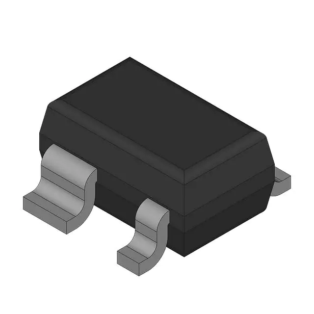
- Part No.:
- BB304CDW-TL-E
- Manufacturer:
- Renesas
- Category:
- Single FETs, MOSFETs
- Package:
- SC-82A, SOT-343
- Datasheet:
-
 BB304CDW-TL-E.pdf
- Description:
- RF MOSFET
- Quantity:
- Payment:

- Shipping:

Inventory:4,046
Please send an inquiry. Send us your inquiry, and we will respond immediately.
Product details
Overview
BB304CDW-TL-E from Renesas Electronics is a VHF RF amplifier MOS FET IC with built-in biasing circuit, designed for 200 MHz signal amplification in compact wireless receivers. It delivers 29 dB typical power gain, 1.2 dB typical noise figure, and operates from 5–9 V supply voltage in a CMPAK-4 (SOT-343mod) package.
For engineers reviewing the BB304CDW-TL-E datasheet, BB304CDW-TL-E pinout, BB304CDW-TL-E application, or BB304CDW-TL-E equivalent, key selection criteria include its dual-gate structure for gain/noise optimization, ESD robustness (200 V HBM), and suitability for low-power VHF front-end stages where board space and component count are constrained.
Technical Context
The BB304CDW-TL-E is a dual-gate silicon N-channel MOSFET optimized for VHF amplification up to 1 GHz. Its gate1 controls DC bias and transconductance, while gate2 provides independent RF signal injection-enabling high isolation (S12 < 0.0053 at 200 MHz) and stable gain control without external bias networks.
It features integrated ESD protection diodes on all terminals and uses a thermally efficient CMPAK-4 package with source-connected die pad for channel temperature management up to 150°C. The device is characterized at 25°C with fixed test conditions including RG = 180 kΩ (5 V) or 470 kΩ (9 V) for reproducible operating point setup.
Key Specifications
| Parameter | Value and Actual Design Meaning |
|---|---|
| Power Gain (PG) | 29 dB typ. at 200 MHz - enables single-stage amplification of weak VHF signals without cascading stages |
| Noise Figure (NF) | 1.2 dB typ. at 200 MHz - preserves signal integrity in receiver front-ends sensitive to thermal noise |
| Supply Voltage Range | 5–9 V - supports direct integration with common logic-supply rails and battery-powered systems |
| Drain Current (ID) | 14 mA typ. at 5 V - sets low quiescent power consumption (~70 mW) for portable applications |
| ESD Withstanding | 200 V HBM (C = 200 pF, Rs = 0 Ω) - eliminates need for external ESD protection in cost-sensitive designs |
| Input Capacitance (Ciss) | 2.8 pF typ. - minimizes loading on preceding filter or antenna matching network |
| Gate Cutoff Voltages | VG1S(off): 0.4–1.0 V; VG2S(off): 0.5–1.0 V - defines usable gate drive range for analog gain control |
Pinout & Package
CMPAK-4 (SOT-343mod) surface-mount package with exposed thermal pad (RENESAS code PTSP0004ZA-A); 4-pin configuration optimized for RF layout with minimal parasitic inductance.
| Pin/Terminal | Circuit Role | Design Meaning |
|---|---|---|
| 1 | Source | Common reference node for both gates and drain; connected to ground plane for RF stability and thermal dissipation |
| 2 | Gate1 | DC bias input controlling transconductance and operating current; requires stable resistive divider or voltage source |
| 3 | Gate2 | RF signal input terminal; high isolation from drain (S12 < 0.005) enables clean signal injection without feedback |
| 4 | Drain | RF output node; matched to 50 Ω system impedance via external L-network per test circuit on page 3 |
Key Features
| Feature | Design Value |
|---|---|
| Built-in biasing circuit | Eliminates external bias resistors and capacitors, reducing BOM count and PCB area by ≥3 components per stage |
| Dual-gate architecture | Enables independent control of DC operating point (Gate1) and RF signal path (Gate2), improving gain stability vs. supply variation |
| Low-noise VHF performance | 1.2 dB NF at 200 MHz meets requirements for FM radio, land-mobile radio, and ISM-band receivers |
| Thermally enhanced package | CMPAK-4's exposed source pad allows direct thermal coupling to PCB ground plane, sustaining 100 mW channel dissipation |
| ESD-protected terminals | Integrated diodes withstand 200 V HBM, enabling handling and assembly without special ESD precautions |
Applications
| FM Radio Receiver Front-End | Land-Mobile Radio IF Amplifier |
|---|---|
Use Scenario: Amplifying weak 88–108 MHz broadcast signals after antenna matching and before mixer stage. IC Role / Device Role / Timing Role: First-stage low-noise amplifier (LNA) providing gain and noise suppression prior to frequency conversion. Use Value: 1.2 dB NF preserves SNR of marginal signals; 29 dB PG reduces need for additional gain stages, lowering system power and complexity. |
Use Scenario: Boosting intermediate-frequency signals (e.g., 45 MHz) in two-way radios used by public safety or commercial fleets. IC Role / Device Role / Timing Role: Fixed-gain IF amplifier ensuring consistent signal level across varying input conditions and temperature ranges. Use Value: Stable 29 dB PG over 5–9 V supply accommodates battery voltage sag; dual-gate structure rejects power supply ripple from adjacent PA stages. |
| ISM Band Sensor Transceiver | Portable TV Tuner Front-End |
Use Scenario: Transmit/receive switching in 315/433 MHz wireless sensor nodes with duty-cycled operation. IC Role / Device Role / Timing Role: Shared LNA/LPF driver supporting bidirectional RF paths with minimal footprint. Use Value: Low 14 mA ID at 5 V extends battery life; ESD tolerance simplifies PCB-level protection design for unshielded IoT enclosures. |
Use Scenario: Signal conditioning in handheld DVB-T tuners receiving VHF band I/III (47–230 MHz) terrestrial broadcasts. IC Role / Device Role / Timing Role: Wideband pre-amplifier compensating for insertion loss of tunable filters and SAW devices. Use Value: 2.8 pF Ciss minimizes detuning of high-Q front-end filters; 5–9 V operation matches USB-powered tuner module supplies. |
Equivalent & Alternatives
The following parts are listed as comparable options for similar VHF RF amplifier applications.
| Alternative Part | Technical Difference | Application Difference | Selection Advice |
|---|---|---|---|
| NE68033 | Single-gate GaAs FET; higher gain (35 dB) but no built-in biasing; requires external gate resistor network | Lacks integrated biasing, increasing component count and layout sensitivity; better suited for fixed-bias, high-performance discrete designs | Select when maximum gain at 200 MHz is critical and board space permits external bias components |
| BF998 | Dual-gate Si MOSFET; similar 28 dB PG and 1.5 dB NF at 200 MHz; wider VDS rating (20 V) but no specified ESD rating | Higher voltage tolerance supports 12 V systems; lacks documented ESD protection, requiring external diodes in harsh environments | Select for 12 V industrial receivers where ESD risk is mitigated by system-level protection |
Compared with NE68033 and BF998, BB304CDW-TL-E uniquely combines dual-gate functionality, built-in biasing, and 200 V HBM ESD protection in a miniature 4-pin package-making it optimal for space-constrained, low-voltage, production-ready VHF amplifiers where BOM reduction and assembly reliability are prioritized.
Availability
BB304CDW-TL-E is available at Aetrix Electronics and suitable for FM radio receivers, land-mobile radios, ISM-band sensor transceivers, and portable TV tuners requiring stable component supply and consistent RF performance across production batches.
Supply support for BB304CDW-TL-E includes scheduled delivery planning, volume procurement assistance, BOM continuity management, traceable sourcing, and lifecycle availability coordination for OEM customers, industrial embedded developers, connected-device designers, and electronics production programs.
Manufacturer
Renesas Electronics Corporation is a global semiconductor leader specializing in microcontrollers, analog, power, and RF solutions for automotive, industrial, and consumer applications.
BB304CDW-TL-E belongs to Renesas' BBFET family of integrated RF MOSFETs designed specifically for cost-sensitive, space-constrained VHF amplification in consumer and professional wireless equipment.
FAQ
What is the primary function of BB304CDW-TL-E in an RF signal chain?
The BB304CDW-TL-E serves as a low-noise, high-gain VHF amplifier-typically deployed as the first active stage in receiver front-ends. Its dual-gate architecture allows independent control of bias (Gate1) and RF input (Gate2), delivering 29 dB typical power gain and 1.2 dB typical noise figure at 200 MHz while minimizing external component count. This makes BB304CDW-TL-E ideal for compact, battery-efficient RF designs where signal integrity and board space are critical.
Does BB304CDW-TL-E require external biasing components?
No-BB304CDW-TL-E integrates a complete biasing circuit, eliminating the need for external gate resistors or bypass capacitors typically required for discrete dual-gate MOSFETs. Gate1 accepts a DC bias voltage (e.g., 5 V via simple resistor divider), while Gate2 receives the RF signal directly. This built-in biasing reduces component count by at least three parts per stage and improves layout reproducibility, as confirmed in the "Features" section of the Renesas BB304C datasheet (Rev. 6.00).
What package type does BB304CDW-TL-E use, and why is it suitable for RF applications?
BB304CDW-TL-E uses the CMPAK-4 (SOT-343mod) package, designated by Renesas as PTSP0004ZA-A. Its 4-pin configuration places Source (Pin 1) and Drain (Pin 4) on opposite corners to minimize loop inductance, while Gate1 (Pin 2) and Gate2 (Pin 3) are adjacent for controlled RF routing. The exposed source pad enhances thermal conduction and RF grounding-critical for stable 200 MHz operation and 100 mW channel dissipation, as detailed in the "Outline" and "Package Dimensions" sections of the datasheet.
How does BB304CDW-TL-E handle electrostatic discharge (ESD)?
BB304CDW-TL-E incorporates built-in ESD-absorbing diodes on all terminals and is rated for 200 V HBM (Human Body Model) with C = 200 pF and Rs = 0 Ω. This level of on-chip protection eliminates the need for external ESD suppressors in most consumer and industrial applications, simplifying PCB layout and reducing BOM cost. The specification is explicitly stated in the "Features" section of the Renesas BB304C datasheet (Rev. 6.00, page 1).
Can BB304CDW-TL-E operate from a 3.3 V supply?
No-BB304CDW-TL-E is specified for 5–9 V operation only. Absolute maximum ratings limit VDS to 12 V and VG1S to +10 V, while electrical characteristics (e.g., ID(op), PG, NF) are guaranteed only at 5 V or 9 V test conditions. At 3.3 V, drain current drops below functional threshold (ID < 5 mA), resulting in insufficient gain and degraded noise performance. Designers must use a minimum 5 V supply, as confirmed in the "Electrical Characteristics" table (page 2) and "Features" list.
BB304CDW-TL-E Specifications
- Product attributes
- Attribute value
- Manufacturer:
- Renesas
- Series:
- -
- Package/Case:
- SC-82A, SOT-343
- Packaging:
- Bulk
- Product Status:
- Not For New Designs
- Technology:
- MOSFET (Metal Oxide)
- Configuration:
- -
- Frequency:
- -
- Gain:
- 29dB
- Voltage - Test:
- 9 V
- Current Rating (Amps):
- 25mA
- Noise Figure:
- 1.2dB
- Current - Test:
- -
- Power - Output:
- -
- Voltage - Rated:
- 12 V
- Grade:
- -
- Qualification:
- -
- Mounting Type:
- Surface Mount
- Supplier Device Package:
- CMPAK-4
BB304CDW-TL-E FAQ
1.How can I place an order for BB304CDW-TL-E through Aetrix?
Please submit a Request for Quotation (RFQ) for BB304CDW-TL-E on Aetrix. Our sales agent will provide a competitive quotation and guide you through the order confirmation once you accept the terms.
2.Are the price and stock information for BB304CDW-TL-E reliable?
The price and inventory of BB304CDW-TL-E are updated periodically and may fluctuate due to market conditions. Stock and pricing data are typically refreshed every 24 hours. Quotation validity for BB304CDW-TL-E is usually 5 days.
3.What payment methods are accepted for BB304CDW-TL-E?
We accept Wire Transfer, PayPal, Credit Card, Western Union, MoneyGram, and Escrow for BB304CDW-TL-E transactions.
Note: Certain payment methods may incur a processing fee.
4.How is shipping managed for BB304CDW-TL-E?
BB304CDW-TL-E orders can be shipped via leading logistics carriers, including DHL, UPS, FedEx, TNT, or Registered Mail.
Once your BB304CDW-TL-E order is processed, you will receive an email with the shipment details and tracking number.
Note: Tracking information may take up to 24 hours to appear. Express delivery typically takes 3–5 business days.
5.How can I obtain technical support or documentation for BB304CDW-TL-E?
For technical support, including BB304CDW-TL-E datasheets, pinout diagrams, or application guidance, please contact our engineering support team. They can provide detailed documentation and assistance for your BB304CDW-TL-E requirements.
6.How does Aetrix verify that BB304CDW-TL-E is sourced from the original manufacturer or authorized distributors?
All BB304CDW-TL-E products on Aetrix are procured from qualified distributors and authorized channels. Our dedicated quality assurance team conducts strict verification, including traceability checks and, if necessary, third-party testing. This ensures that BB304CDW-TL-E meets industry standards.
7.What is the process for return or replacement of BB304CDW-TL-E?
All BB304CDW-TL-E units undergo pre-shipment inspection (PSI). If there is an issue with BB304CDW-TL-E, returns or replacements are accepted under the following conditions:
1.Quantity discrepancies, incorrect items, or visible external defects (such as breakage or corrosion), acknowledged by Aetrix.
2.The issue is reported within 90 days of delivery.
3.The BB304CDW-TL-E part is unused and in its original packaging.
Return procedure for BB304CDW-TL-E:
1.Submit a request within 90 days.
2.Obtain a Return Material Authorization (RMA) from Aetrix.
BB304CDW-TL-E Tags
-
3SK294(TE85L,F)
Toshiba Semiconductor and Storage

-
SAV-551+
Mini-Circuits

-
TAV2-501+
Mini-Circuits
-
CE3514M4-C2
CEL
-
AFT05MS004NT1
NXP USA Inc.
-
SAV-541+
Mini-Circuits
-
CE3512K2-C1
CEL
-
AFM907NT1
NXP Semiconductors
-
SKY65050-372LF
Skyworks Solutions Inc.
-
CE3520K3-C1
CEL
-
AFT09MS007NT1
NXP USA Inc.
-
AFT09MS015NT1
NXP USA Inc.
Tech Hub

TTL and CMOS logic families differ in thresholds, loading, output drive, power and timing. This engineering guide compares 74HC and 74HCT, calculates noise margins and checks 3.3 V/5 V compatibility.

A practical engineering guide to 3.3V and 5V logic compatibility, input thresholds, resistor dividers, translator ICs, MOSFET level shifting, I2C pull-ups, timing limits and power-sequencing risks.

The 74HC595 uses push-pull logic outputs, while the TPIC6B595 uses 50 V open-drain DMOS sinks for higher-power loads. This guide compares timing, current limits, 3.3 V interfacing, load wiring, thermal…

The 74HC595 converts serial data into eight stable parallel outputs. This guide covers pin functions, shift and storage timing, OE and MR behavior, drive-current limits, cascading, voltage compatibilit…

A technical comparison of level-sensitive latches and edge-triggered flip-flops, covering timing windows, setup and hold limits, master–slave operation, time borrowing, race-through, HDL inference and…

A D latch stores one bit while Enable controls when data can pass. This reference covers gate-level operation, truth tables, transparency, setup and hold timing, LE versus OE, common ICs and practical …

An SR latch stores one bit through cross-coupled feedback. This engineering reference covers NOR and NAND implementations, truth tables, forbidden-state recovery, gated operation, switch debouncing, fa…

Latch circuits retain one bit through feedback. This technical reference covers SR and D latches, truth tables, transparency, timing limits, latch-versus-flip-flop behavior, applications and common log…

An engineering guide to LED driver operation, constant-current and constant-voltage outputs, linear and switching topologies, dimming, IC selection, calculations, replacement compatibility, and fault c…

Operational amplifier guide covering op amp basics, feedback, ideal vs real op amps, common configurations, buffer circuits, offset, bias current, gain-bandwidth, slew rate, rail-to-rail limits and sel…


