
 My Inquiry
 My Account


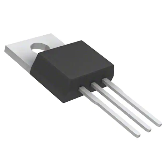
onsemi BDW93CTU
- Part No.:
- BDW93CTU
- Manufacturer:
- onsemi
- Category:
- Single Bipolar Transistors
- Package:
- TO-220-3
- Datasheet:
-
 BDW93CTU.pdf
- Description:
- TRANS NPN DARL 100V 12A TO-220-3
- Quantity:
- Payment:

- Shipping:

Inventory:4,390
Please send an inquiry. Send us your inquiry, and we will respond immediately.
Product details
Overview
BDW93CTU from ON Semiconductor is a high-power NPN epitaxial silicon Darlington transistor in TO-220 package, rated for 100 V VCEO, 12 A DC collector current, and 80 W power dissipation at TC = 25°C. It delivers hFE ≥ 100 at IC = 10 A and features integrated parallel diode with VF ≤ 1.8 V at IF = 10 A, used in industrial hammer drivers and audio amplifier output stages.
For engineers reviewing the BDW93CTU datasheet, pinout, applications, or equivalent options, key selection criteria include VCEO rating, safe operating area (SOA) at high pulse currents, thermal resistance (RθJC = 1.5°C/W), and complementary pairing with BDW94CTU for push-pull configurations.
Technical Context
The BDW93CTU implements a monolithic Darlington pair with built-in base-emitter shunt resistor and parallel freewheeling diode, enabling direct drive of inductive loads without external flyback protection. Its SOA curve supports 100 V × 10 A operation for 100 µs pulses and maintains stable gain (hFE = 100–20,000) across 0.1–10 A collector current range.
Designed for linear and switching operation, it uses epitaxial base construction to minimize saturation voltage (VCE(sat) ≤ 3 V at IC = 10 A, IB = 100 mA) and withstands VCBO = 100 V. Thermal derating begins at TC = 25°C, with full power maintained up to 100°C case temperature per the published derating curve.
Key Specifications
| Parameter | Value and Actual Design Meaning |
|---|---|
| VCEO | 100 V - Maximum continuous collector-emitter voltage before breakdown; defines upper rail limit in amplifier or driver stage |
| IC (DC) | 12 A - Sustained collector current capability; determines heatsink sizing for continuous conduction |
| PC | 80 W at TC = 25°C - Total power dissipation limit; requires thermal interface design to maintain junction below 150°C |
| hFE | 100 min at IC = 10 A - Minimum DC current gain; sets required base drive current for full-load switching |
| RθJC | 1.5°C/W - Junction-to-case thermal resistance; enables calculation of case temperature rise under load |
| VF (diode) | ≤ 1.8 V at IF = 10 A - Forward voltage of integrated parallel diode; limits power loss during inductive flyback |
Pinout & Package
BDW93CTU is housed in a standard TO-220 package with insulated tab, 3-pin configuration, and through-hole mounting. The case serves as the collector terminal and must be electrically isolated from heatsink unless system grounding permits common-collector connection.
| Pin/Terminal | Circuit Role | Design Meaning |
|---|---|---|
| 1 (Left) | Base | Control input requiring ~100 mA base current to saturate at 10 A collector load |
| 2 (Center) | Collector | Main power terminal; electrically connected to metal tab; requires isolation if heatsink is grounded |
| 3 (Right) | Emitter | Power return path; referenced to ground or negative rail in common-emitter configurations |
Key Features
| Feature | Design Value |
|---|---|
| Integrated freewheeling diode | Reduces external component count in relay/hammer driver circuits by providing inherent inductive kickback path |
| Monolithic Darlington structure | Delivers high current gain (hFE ≥ 100 at 10 A) without discrete cascading, simplifying base drive design |
| 100 V VCEO rating | Supports operation in 48 V and 72 V industrial bus systems with margin for transient overvoltage |
| TO-220 mechanical standardization | Enables drop-in replacement in legacy designs using industry-standard footprint and mounting holes |
Applications
| Industrial Hammer Drivers | Audio Power Amplifiers |
|---|---|
Use Scenario: Driving solenoid-based impact hammers in automated riveting or stamping equipment with 10–100 ms on-time pulses. IC Role / Device Role / Timing Role: High-current switch controlling solenoid coil energization; operates in saturated switching mode with fast turn-off via base discharge. Use Value: Integrated diode clamps inductive flyback energy, eliminating need for external TVS or snubber, reducing BOM count and PCB area. | Use Scenario: Output stage in Class AB audio amplifiers delivering ≥50 W into 4 Ω or 8 Ω loads. IC Role / Device Role / Timing Role: Final power gain element handling peak output currents >8 A; biased in linear region with thermal feedback. Use Value: Low VCE(sat) (≤3 V) minimizes conduction loss at full output, improving efficiency and reducing heatsink requirements. |
| DC Motor Controllers | Power Supply Regulators |
Use Scenario: H-bridge low-side switch in brushed DC motor control for conveyor systems or robotic joints. IC Role / Device Role / Timing Role: High-current sinking switch; paired with complementary BDW94CTU for bidirectional control. Use Value: Matched VCEO and hFE specs ensure symmetrical performance in push-pull topology, minimizing shoot-through risk. | Use Scenario: Pass transistor in linear regulated power supplies delivering up to 10 A at adjustable output voltages. IC Role / Device Role / Timing Role: Series pass element dissipating excess input-output differential voltage; operated in active region. Use Value: High PC (80 W) and low RθJC (1.5°C/W) enable stable regulation under worst-case dropout conditions without thermal runaway. |
Equivalent & Alternatives
The following parts are listed as comparable options for similar high-power NPN Darlington transistor applications.
| Alternative Part | Technical Difference | Application Difference | Selection Advice |
|---|---|---|---|
| BDW93C | Same die and electrical specs; non-TU suffix indicates tape-and-reel vs. tube packaging | No functional difference; TU denotes tube packaging per ON Semiconductor ordering convention | Select BDW93CTU when tube packaging is required for manual prototyping or low-volume assembly |
| MJD127G | Lower VCEO (80 V), lower IC (8 A), TO-252 surface-mount package, no integrated diode | Suitable only for ≤48 V systems; requires external flyback diode and re-layout for SMT placement | Choose MJD127G only if board space constraints mandate SMT and voltage/current demands are reduced |
Compared with BDW93CTU, BDW93C offers identical performance in tube packaging, while MJD127G trades voltage/current headroom and integrated protection for surface-mount compatibility-neither is pin-compatible, and layout changes are required for either alternative.
Availability
BDW93CTU is available at Aetrix Electronics and suitable for industrial hammer drivers, audio power amplifiers, and DC motor controllers requiring stable component supply, long-lifecycle support, and consistent parametric performance across production batches.
Supply support for BDW93CTU includes scheduled delivery planning, volume procurement assistance, BOM continuity management, traceable sourcing, and lifecycle availability coordination for OEM customers, industrial embedded developers, connected-device designers, and electronics production programs.
Manufacturer
ON Semiconductor is a global semiconductor manufacturer specializing in power management, analog, sensor, and logic devices for automotive, industrial, and cloud power applications.
The BDW93CTU belongs to ON Semiconductor's legacy high-power bipolar transistor product line, originally developed by Fairchild Semiconductor for ruggedized linear and switching power control in factory automation and audio systems.
FAQ
What is the maximum continuous collector current rating for BDW93CTU?
The BDW93CTU has a maximum continuous collector current (IC) rating of 12 A at TC = 25°C. This rating assumes adequate heatsinking to maintain case temperature within limits; derating applies above 25°C per the published thermal curve. At 100°C case temperature, usable IC drops to approximately 6 A. BDW93CTU must not be operated beyond its Safe Operating Area boundaries defined in the datasheet.
Does BDW93CTU include an integrated freewheeling diode?
Yes, BDW93CTU integrates a parallel freewheeling diode between collector and emitter, with forward voltage VF ≤ 1.8 V at IF = 10 A. This diode provides inherent protection against inductive kickback in relay, solenoid, and motor drive applications. No external flyback diode is required when using BDW93CTU in such topologies, reducing component count and failure points.
What is the pin configuration of BDW93CTU in the TO-220 package?
BDW93CTU uses a standard TO-220 3-pin configuration: Pin 1 (left) is Base, Pin 2 (center) is Collector (connected to the metal tab), and Pin 3 (right) is Emitter. The tab is electrically live as the collector terminal and must be insulated from the heatsink unless system grounding architecture permits direct contact. Mounting orientation follows JEDEC TO-220 outline standards.
How does BDW93CTU differ from BDW93A and BDW93B variants?
BDW93CTU differs from BDW93A and BDW93B primarily in its voltage ratings: BDW93CTU has VCEO = 100 V and VCBO = 100 V, whereas BDW93A is rated for 60 V and BDW93B for 80 V. All share identical package (TO-220), current rating (12 A), power dissipation (80 W), and internal Darlington/diode structure. Selection depends strictly on required voltage margin in the target application.
Is BDW93CTU suitable for linear regulator applications?
Yes, BDW93CTU is suitable for linear regulator pass transistor applications due to its high power dissipation (80 W), low thermal resistance (RθJC = 1.5°C/W), and stable hFE across operating current. It supports output currents up to 10 A with appropriate heatsinking and biasing. However, designers must verify SOA compliance under worst-case dropout and load conditions, as BDW93CTU is not internally current-limited.
BDW93CTU Specifications
- Product attributes
- Attribute value
- Manufacturer:
- onsemi
- Series:
- -
- Package/Case:
- TO-220-3
- Packaging:
- Tube
- Product Status:
- Obsolete
- Transistor Type:
- NPN - Darlington
- Current - Collector (Ic) (Max):
- 12 A
- Voltage - Collector Emitter Breakdown (Max):
- 100 V
- Vce Saturation (Max) @ Ib, Ic:
- 3V @ 100mA, 10A
- Current - Collector Cutoff (Max):
- 1mA
- DC Current Gain (hFE) (Min) @ Ic, Vce:
- 750 @ 5A, 3V
- Power - Max:
- 80 W
- Frequency - Transition:
- -
- Operating Temperature:
- 150°C (TJ)
- Grade:
- -
- Qualification:
- -
- Mounting Type:
- Through Hole
- Supplier Device Package:
- TO-220-3
BDW93CTU FAQ
1.How can I place an order for BDW93CTU through Aetrix?
Please submit a Request for Quotation (RFQ) for BDW93CTU on Aetrix. Our sales agent will provide a competitive quotation and guide you through the order confirmation once you accept the terms.
2.Are the price and stock information for BDW93CTU reliable?
The price and inventory of BDW93CTU are updated periodically and may fluctuate due to market conditions. Stock and pricing data are typically refreshed every 24 hours. Quotation validity for BDW93CTU is usually 5 days.
3.What payment methods are accepted for BDW93CTU?
We accept Wire Transfer, PayPal, Credit Card, Western Union, MoneyGram, and Escrow for BDW93CTU transactions.
Note: Certain payment methods may incur a processing fee.
4.How is shipping managed for BDW93CTU?
BDW93CTU orders can be shipped via leading logistics carriers, including DHL, UPS, FedEx, TNT, or Registered Mail.
Once your BDW93CTU order is processed, you will receive an email with the shipment details and tracking number.
Note: Tracking information may take up to 24 hours to appear. Express delivery typically takes 3–5 business days.
5.How can I obtain technical support or documentation for BDW93CTU?
For technical support, including BDW93CTU datasheets, pinout diagrams, or application guidance, please contact our engineering support team. They can provide detailed documentation and assistance for your BDW93CTU requirements.
6.How does Aetrix verify that BDW93CTU is sourced from the original manufacturer or authorized distributors?
All BDW93CTU products on Aetrix are procured from qualified distributors and authorized channels. Our dedicated quality assurance team conducts strict verification, including traceability checks and, if necessary, third-party testing. This ensures that BDW93CTU meets industry standards.
7.What is the process for return or replacement of BDW93CTU?
All BDW93CTU units undergo pre-shipment inspection (PSI). If there is an issue with BDW93CTU, returns or replacements are accepted under the following conditions:
1.Quantity discrepancies, incorrect items, or visible external defects (such as breakage or corrosion), acknowledged by Aetrix.
2.The issue is reported within 90 days of delivery.
3.The BDW93CTU part is unused and in its original packaging.
Return procedure for BDW93CTU:
1.Submit a request within 90 days.
2.Obtain a Return Material Authorization (RMA) from Aetrix.
BDW93CTU Tags
-
MMBT3906LT1G
onsemi
-
MMBT3904-7-F
Diodes Incorporated
-
MMBT3904LT1G
onsemi
-
MMBT3906-7-F
Diodes Incorporated
-
MMBT3904-TP
Micro Commercial Co
-
MMBT2222A-7-F
Diodes Incorporated
-
BC846BLT1G
onsemi
-
BC847B,215
Nexperia USA Inc.
-
SMMBT3904LT1G
onsemi
-
MMBT2222A-TP
Micro Commercial Co
-
MMBTA06LT1G
onsemi
-
MMBT2222ALT1G
onsemi
Tech Hub

Counterfeit components can hide behind convincing markings and passing basic function tests. This engineering reference covers source traceability, external inspection, X-ray, XRF, electrical testing, …

A practical engineering and sourcing framework covering lifecycle verification, lifetime-buy calculations, replacement qualification, supplier checks and counterfeit-risk controls.

TTL and CMOS logic families differ in thresholds, loading, output drive, power and timing. This engineering guide compares 74HC and 74HCT, calculates noise margins and checks 3.3 V/5 V compatibility.

A practical engineering guide to 3.3V and 5V logic compatibility, input thresholds, resistor dividers, translator ICs, MOSFET level shifting, I2C pull-ups, timing limits and power-sequencing risks.

The 74HC595 uses push-pull logic outputs, while the TPIC6B595 uses 50 V open-drain DMOS sinks for higher-power loads. This guide compares timing, current limits, 3.3 V interfacing, load wiring, thermal…

The 74HC595 converts serial data into eight stable parallel outputs. This guide covers pin functions, shift and storage timing, OE and MR behavior, drive-current limits, cascading, voltage compatibilit…

A technical comparison of level-sensitive latches and edge-triggered flip-flops, covering timing windows, setup and hold limits, master–slave operation, time borrowing, race-through, HDL inference and…

A D latch stores one bit while Enable controls when data can pass. This reference covers gate-level operation, truth tables, transparency, setup and hold timing, LE versus OE, common ICs and practical …

An SR latch stores one bit through cross-coupled feedback. This engineering reference covers NOR and NAND implementations, truth tables, forbidden-state recovery, gated operation, switch debouncing, fa…

Latch circuits retain one bit through feedback. This technical reference covers SR and D latches, truth tables, transparency, timing limits, latch-versus-flip-flop behavior, applications and common log…


