
 My Inquiry
 My Account


NXP Semiconductors BF1205,115
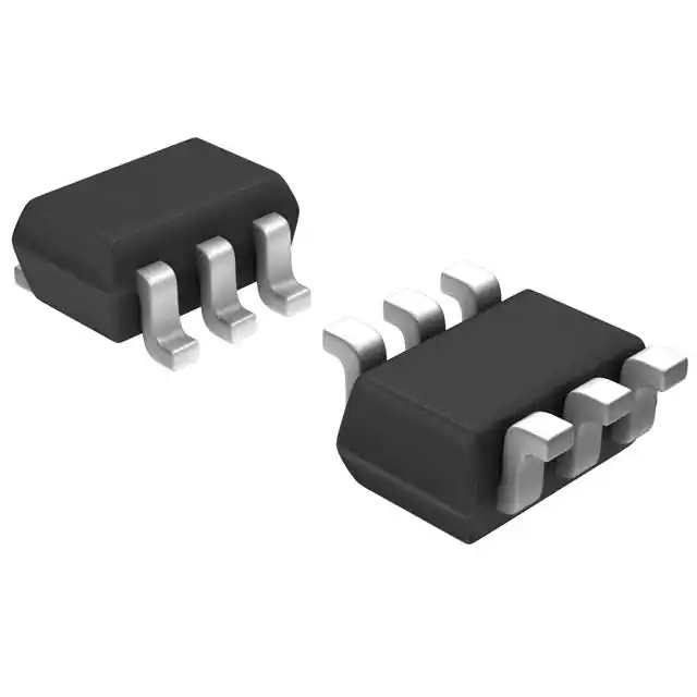
- Part No.:
- BF1205,115
- Manufacturer:
- NXP Semiconductors
- Category:
- Single FETs, MOSFETs
- Package:
- 6-TSSOP, SC-88, SOT-363
- Datasheet:
-
 BF1205,115.pdf
- Description:
- RF MOSFET 5V 6TSSOP
- Quantity:
- Payment:

- Shipping:

Inventory:5,682
Please send an inquiry. Send us your inquiry, and we will respond immediately.
Product details
Overview
BF1205 from NXP Semiconductors is a dual N-channel dual-gate MOSFET in SOT363 package, integrating two low-noise amplifiers with shared source and gate-2 leads plus an internal AGC-controlled switch. It delivers 31 mS forward transfer admittance, 1.2–1.4 dB noise figure at 800 MHz, and >98 dBµV cross-modulation rejection at 40 dB AGC, enabling VHF/UHF gain-controlled LNA stages in 5 V TV tuners and professional comms equipment.
For engineers reviewing the BF1205 datasheet, BF1205 pinout, BF1205 application, or BF1205 equivalent, key selection criteria include dual-gate noise performance at UHF, integrated switching for AGC path control, gate-1 bias-dependent amplifier enable/disable behavior, and SOT363 footprint compatibility with high-density RF front-end layouts.
Technical Context
The BF1205 implements two matched dual-gate MOSFETs (Amplifier A and B) sharing source (Pin 5) and gate-2 (Pin 2), with independent gate-1 inputs (Pins 1 and 3). Amplifier B's gate-1 (Pin 3) controls the internal switch that enables/disables Amplifier A - VGG = 0 V activates Amp A while deactivating Amp B, and VGG = 5 V reverses this state per Fig.4.
Each amplifier operates in common-source configuration with fully or partly integrated DC bias networks. Integrated protection diodes clamp gate-to-source surges, and substrate-source interconnection ensures stable RF grounding. Thermal resistance is 240 K/W junction-to-soldering-point, with 200 mW total power dissipation derated above Ts = 102 °C.
Key Specifications
| Parameter | Value and Actual Design Meaning |
|---|---|
| VDS max | 10 V - supports 5 V supply rails with margin for transient spikes in tuner front-ends |
| |yfs| typ | 31 mS - high transconductance enables strong small-signal gain at UHF frequencies |
| NF @ 800 MHz | 1.2 dB (Amp A), 1.4 dB (Amp B) - meets stringent low-noise requirements for digital TV reception |
| Xmod @ 40 dB AGC | 98–105 dBµV - superior cross-modulation suppression critical for multi-channel VHF/UHF signal integrity |
| Ciss (Gate 1) | 1.8–2.5 pF - ultra-low input capacitance minimizes loading on preceding RF filters or mixers |
| Ptot max | 200 mW - sufficient for continuous-wave LNA operation in compact SOT363 package |
| Rth j-s | 240 K/W - defines thermal design boundary for PCB copper area and solder joint reliability |
Pinout & Package
Encapsulated in SOT363 - a 6-lead micro-miniature plastic surface-mount package (2.2 × 1.35 × 1.15 mm) with gull-wing leads, optimized for RF layout and reflow compatibility.
| Pin/Terminal | Circuit Role | Design Meaning |
|---|---|---|
| 1 | Gate 1 (Amplifier A) | Primary AGC control input for Amp A; referenced to source (Pin 5); voltage-tunable gain |
| 2 | Gate 2 (Shared) | Common RF input for both amplifiers; connected internally to same node |
| 3 | Gate 1 (Amplifier B) | VGG control terminal: sets operating state of internal switch (0 V → Amp A ON / 5 V → Amp B ON) |
| 4 | Drain (Amplifier B) | RF output node for Amp B; requires external matching network for 50 Ω system interface |
| 5 | Source (Shared) | Common source and substrate connection; must be low-inductance RF ground in layout |
| 6 | Drain (Amplifier A) | RF output node for Amp A; independent of Amp B drain; requires separate output matching |
Key Features
| Feature | Design Value |
|---|---|
| Dual independent LNAs in one package | Reduces board space and component count vs. discrete dual-LNA solutions; eliminates inter-device matching variance |
| Integrated AGC switch | Eliminates need for external analog switch or relay; enables seamless gain switching without added insertion loss or timing skew |
| Shared gate-2 and source | Ensures identical RF input path and DC bias conditions for both amplifiers, improving channel-to-channel consistency |
| Internal gate protection diodes | Withstands ESD events up to ±10 mA gate current without external clamping components |
| High yfs/Ciss ratio | Delivers high gain per unit input capacitance - preserves Q-factor of tuned input circuits in narrowband VHF applications |
Applications
| Analog TV Tuner Front-End | Digital Terrestrial TV (DTT) Tuner |
|---|---|
Use Scenario: Low-noise amplification of VHF/UHF broadcast signals prior to mixer stage in consumer TV receivers. IC Role / Device Role / Timing Role: Dual-gate MOSFET LNA with AGC-controlled gain switching between antenna diversity paths. Use Value: 1.2 dB NF at 800 MHz and >98 dBµV cross-modulation rejection ensure robust reception under weak-signal and co-channel interference conditions. | Use Scenario: Gain-controlled RF amplification in DTT set-top boxes supporting DVB-T/T2 standards across 47–862 MHz band. IC Role / Device Role / Timing Role: Dual-path LNA enabling dynamic range optimization during channel scanning and signal lock acquisition. Use Value: Integrated switch allows real-time path selection without external control logic, reducing system latency and BOM cost. |
| Professional UHF Wireless Microphone Receiver | Land Mobile Radio (LMR) Transceiver Front-End |
Use Scenario: High-linearity, low-noise receive amplification in battery-powered wireless audio systems operating in 500–900 MHz bands. IC Role / Device Role / Timing Role: Primary LNA with AGC-driven gain reduction to handle wide dynamic range of microphone signal levels. Use Value: 31 mS |yfs| and 26 dB power gain at 400 MHz provide sufficient headroom before mixer compression while maintaining SNR. | Use Scenario: Receive-path amplification in portable LMR radios requiring high sensitivity and adjacent-channel rejection. IC Role / Device Role / Timing Role: Dual-gate LNA configured for optimal noise figure and IP3 trade-off in 136–174 MHz or 400–520 MHz bands. Use Value: Shared gate-2 architecture simplifies input filter design and improves repeatability across production units. |
Equivalent & Alternatives
The following parts are listed as comparable options for similar dual-gate LNA applications.
| Alternative Part | Technical Difference | Application Difference | Selection Advice |
|---|---|---|---|
| BF1204,115 | Single dual-gate MOSFET (no integrated switch); identical SOT363 package and core LNA specs | Lacks internal AGC switching - requires external analog switch or discrete FET for gain control | Select when only one LNA path is needed or when external switching provides greater flexibility |
| MRF9011LT1G | Single-gate GaAs FET; higher fT (12 GHz), lower NF (0.8 dB @ 900 MHz), but no dual-gate AGC capability | Superior noise and gain at higher frequencies, but lacks inherent gain-control mechanism - AGC must be implemented externally | Select for ultra-low-noise fixed-gain UHF amplification where AGC is handled at IF or baseband level |
Compared with BF1204,115, the BF1205 adds integrated switching for automatic path selection, reducing component count and layout complexity. Against MRF9011LT1G, it trades some NF and frequency headroom for built-in dual-gate AGC functionality essential in tuner architectures.
Availability
BF1205 is available at Aetrix Electronics and suitable for analog/digital TV tuners, professional UHF wireless receivers, and land mobile radio front-ends requiring stable component supply, consistent RF performance, and long-term obsolescence management.
Supply support for BF1205 includes scheduled delivery planning, volume procurement assistance, BOM continuity management, traceable sourcing, and lifecycle availability coordination for OEM customers, industrial embedded developers, connected-device designers, and electronics production programs.
Manufacturer
NXP Semiconductors is a global semiconductor company specializing in high-performance RF, analog, and mixed-signal solutions for automotive, industrial, and consumer applications.
The BF1205 belongs to NXP's legacy RF transistor portfolio designed specifically for VHF/UHF gain-controlled low-noise amplification in broadcast and professional communications equipment.
FAQ
What is the maximum drain-source voltage rating for the BF1205?
The BF1205 has a maximum drain-source voltage (VDS) rating of 10 V per MOSFET, as specified in the Absolute Maximum Ratings table. This rating applies independently to both Amplifier A and Amplifier B, allowing safe operation with standard 5 V supply rails while accommodating transient overvoltage conditions typical in RF front-end environments. Exceeding 10 V risks permanent device damage.
How does the internal switch in the BF1205 operate between the two amplifiers?
The internal switch in the BF1205 is controlled by the gate-1 voltage of Amplifier B (Pin 3, labeled VGG). When VGG = 0 V, Amplifier A is enabled and Amplifier B is disabled; when VGG = 5 V, Amplifier B is enabled and Amplifier A is disabled. This complementary switching behavior is defined in Fig.4 and enables seamless AGC-driven path selection without external control circuitry - a core functional distinction of the BF1205 versus single-amplifier dual-gate MOSFETs like the BF1204,115.
What is the typical noise figure of the BF1205 at 800 MHz?
The BF1205 achieves a typical noise figure (NF) of 1.2 dB for Amplifier A and 1.4 dB for Amplifier B at 800 MHz, measured under standard conditions (VDS = 5 V, VG2-S = 4 V, ID = 12 mA). These values are confirmed in the Dynamic Characteristics sections for each amplifier and reflect its suitability for demanding UHF reception applications such as digital terrestrial television tuners where sub-1.5 dB NF is critical for weak-signal performance.
Can the BF1205 be used with a 3.3 V supply instead of 5 V?
The BF1205 is characterized and optimized for 5 V operation, and its Quick Reference Data and Dynamic Characteristics assume VDS = 5 V. While static parameters like V(BR)DSS (min 7–10 V) suggest possible 3.3 V use, gain (Gtr), noise figure, and cross-modulation performance degrade significantly below 5 V due to reduced transconductance and altered bias points. NXP does not specify or guarantee performance at 3.3 V; therefore, BF1205 should be operated at 5 V for full compliance with published specifications.
What package type is the BF1205 supplied in, and what are its key mechanical dimensions?
The BF1205 is supplied in the SOT363 plastic surface-mounted package - also known as SC-88 - with 6 gull-wing leads. Its nominal dimensions are 2.2 mm × 1.35 mm × 1.15 mm (L × W × H), lead pitch of 0.65 mm, and thermal resistance Rth j-s = 240 K/W. The package outline conforms to JEDEC MO-203 and IEC 60191 standards, and the marking code "L4-" appears on the top surface for traceability.
BF1205,115 Specifications
- Product attributes
- Attribute value
- Manufacturer:
- NXP Semiconductors
- Series:
- -
- Package/Case:
- 6-TSSOP, SC-88, SOT-363
- Packaging:
- Tape & Reel (TR)
- Product Status:
- Obsolete
- Technology:
- MOSFET (Metal Oxide)
- Configuration:
- N-Channel Dual Gate
- Frequency:
- 800MHz
- Gain:
- 26dB
- Voltage - Test:
- 5 V
- Current Rating (Amps):
- 30mA
- Noise Figure:
- 1.2dB
- Current - Test:
- 12 mA
- Power - Output:
- -
- Voltage - Rated:
- 10 V
- Grade:
- -
- Qualification:
- -
- Mounting Type:
- Surface Mount
- Supplier Device Package:
- 6-TSSOP
BF1205,115 FAQ
1.How can I place an order for BF1205,115 through Aetrix?
Please submit a Request for Quotation (RFQ) for BF1205,115 on Aetrix. Our sales agent will provide a competitive quotation and guide you through the order confirmation once you accept the terms.
2.Are the price and stock information for BF1205,115 reliable?
The price and inventory of BF1205,115 are updated periodically and may fluctuate due to market conditions. Stock and pricing data are typically refreshed every 24 hours. Quotation validity for BF1205,115 is usually 5 days.
3.What payment methods are accepted for BF1205,115?
We accept Wire Transfer, PayPal, Credit Card, Western Union, MoneyGram, and Escrow for BF1205,115 transactions.
Note: Certain payment methods may incur a processing fee.
4.How is shipping managed for BF1205,115?
BF1205,115 orders can be shipped via leading logistics carriers, including DHL, UPS, FedEx, TNT, or Registered Mail.
Once your BF1205,115 order is processed, you will receive an email with the shipment details and tracking number.
Note: Tracking information may take up to 24 hours to appear. Express delivery typically takes 3–5 business days.
5.How can I obtain technical support or documentation for BF1205,115?
For technical support, including BF1205,115 datasheets, pinout diagrams, or application guidance, please contact our engineering support team. They can provide detailed documentation and assistance for your BF1205,115 requirements.
6.How does Aetrix verify that BF1205,115 is sourced from the original manufacturer or authorized distributors?
All BF1205,115 products on Aetrix are procured from qualified distributors and authorized channels. Our dedicated quality assurance team conducts strict verification, including traceability checks and, if necessary, third-party testing. This ensures that BF1205,115 meets industry standards.
7.What is the process for return or replacement of BF1205,115?
All BF1205,115 units undergo pre-shipment inspection (PSI). If there is an issue with BF1205,115, returns or replacements are accepted under the following conditions:
1.Quantity discrepancies, incorrect items, or visible external defects (such as breakage or corrosion), acknowledged by Aetrix.
2.The issue is reported within 90 days of delivery.
3.The BF1205,115 part is unused and in its original packaging.
Return procedure for BF1205,115:
1.Submit a request within 90 days.
2.Obtain a Return Material Authorization (RMA) from Aetrix.
BF1205,115 Tags
-
3SK294(TE85L,F)
Toshiba Semiconductor and Storage

-
SAV-551+
Mini-Circuits

-
TAV2-501+
Mini-Circuits
-
CE3514M4-C2
CEL
-
AFT05MS004NT1
NXP USA Inc.
-
SAV-541+
Mini-Circuits
-
CE3512K2-C1
CEL
-
AFM907NT1
NXP Semiconductors
-
SKY65050-372LF
Skyworks Solutions Inc.
-
CE3520K3-C1
CEL
-
AFT09MS007NT1
NXP USA Inc.
-
AFT09MS015NT1
NXP USA Inc.
Tech Hub

A practical engineering guide to 3.3V and 5V logic compatibility, input thresholds, resistor dividers, translator ICs, MOSFET level shifting, I2C pull-ups, timing limits and power-sequencing risks.

The 74HC595 uses push-pull logic outputs, while the TPIC6B595 uses 50 V open-drain DMOS sinks for higher-power loads. This guide compares timing, current limits, 3.3 V interfacing, load wiring, thermal…

The 74HC595 converts serial data into eight stable parallel outputs. This guide covers pin functions, shift and storage timing, OE and MR behavior, drive-current limits, cascading, voltage compatibilit…

A technical comparison of level-sensitive latches and edge-triggered flip-flops, covering timing windows, setup and hold limits, master–slave operation, time borrowing, race-through, HDL inference and…

A D latch stores one bit while Enable controls when data can pass. This reference covers gate-level operation, truth tables, transparency, setup and hold timing, LE versus OE, common ICs and practical …

An SR latch stores one bit through cross-coupled feedback. This engineering reference covers NOR and NAND implementations, truth tables, forbidden-state recovery, gated operation, switch debouncing, fa…

Latch circuits retain one bit through feedback. This technical reference covers SR and D latches, truth tables, transparency, timing limits, latch-versus-flip-flop behavior, applications and common log…

An engineering guide to LED driver operation, constant-current and constant-voltage outputs, linear and switching topologies, dimming, IC selection, calculations, replacement compatibility, and fault c…

Operational amplifier guide covering op amp basics, feedback, ideal vs real op amps, common configurations, buffer circuits, offset, bias current, gain-bandwidth, slew rate, rail-to-rail limits and sel…

Jumper cables guide covering safe connection order, red and black clamp placement, final ground connection, cable gauge, length, clamp quality, copper vs CCA cables, jump starter comparison and battery…


