
 My Inquiry
 My Account


NXP Semiconductors BGD704,112
- Part No.:
- BGD704,112
- Manufacturer:
- NXP Semiconductors
- Category:
- Video Amps and Modules
- Package:
- SOT-115J
- Datasheet:
-
 BGD704,112.pdf
- Description:
- IC AMP CATV SOT115J
- Quantity:
- Payment:

- Shipping:

Inventory:4,736
Please send an inquiry. Send us your inquiry, and we will respond immediately.
Product details
Overview
BGD704,112 from NXP Semiconductors is a hybrid RF power doubler amplifier module designed for CATV distribution systems, delivering 20 dB typical gain across 40–750 MHz with 24 V DC supply, 425–435 mA total current draw, and optimized 75 Ω input/output impedance for cable infrastructure signal boosting.
For engineers reviewing the BGD704,112 datasheet, BGD704,112 pinout, BGD704,112 application, or BGD704,112 equivalent, this module is selected for high-linearity, low-noise broadband amplification in headend and node-level CATV signal conditioning where composite distortion (CTB/Xmod/CSO) and flat frequency response are critical design constraints.
Technical Context
This hybrid amplifier integrates silicon nitride passivation and gold metallization for reliability under continuous RF stress in temperature-controlled CATV environments. It operates at 24 V DC with transient tolerance up to 30 V and maintains ±0.2 dB typical flatness from 40 MHz to 750 MHz under 75 Ω matched conditions.
Its architecture delivers 20–21 dB power gain across the full band, with input/output return losses ≥16 dB (typical ≥21 dB) and noise figure ≤5 dB at 50 MHz - enabling cascaded multi-stage amplification while meeting stringent CTB (−58 dB), Xmod (−63 dB), and CSO (−61 dB) requirements for 110-channel flat operation.
Key Specifications
| Parameter | Value and Actual Design Meaning |
|---|---|
| Frequency Range | 40 MHz to 750 MHz - supports full DOCSIS 3.1/4.0 upstream/downstream spectrum in HFC networks. |
| Power Gain | 20 dB typ. @ 50 MHz and 21 dB typ. @ 750 MHz - enables consistent signal boost across entire CATV band. |
| Noise Figure | 4.5 dB typ. @ 50 MHz, 6.5 dB typ. @ 750 MHz - preserves upstream SNR in multi-drop coaxial trees. |
| Composite Distortion | CTB −58 dB, Xmod −63 dB, CSO −61 dB @ 110 channels - meets FCC Part 76 linearity mandates. |
| Current Consumption | 425–435 mA @ 24 V - defines thermal load and power supply sizing for rack-mounted amplifiers. |
| Input/Output Impedance | 75 Ω - direct interface with standard CATV coaxial infrastructure without matching networks. |
| Flatness | ±0.2 dB typ. over 40–750 MHz - eliminates need for external equalization in wideband nodes. |
Pinout & Package
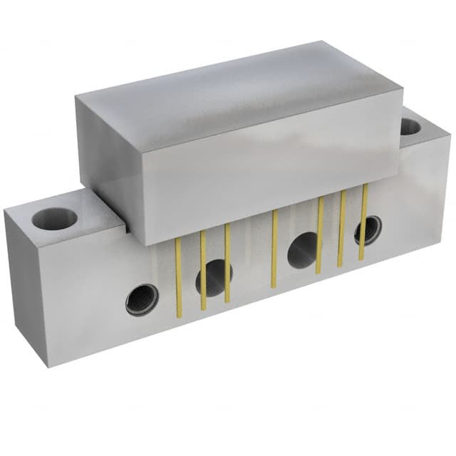
SOT115J package: rectangular single-ended aluminum flange with 2 vertical and 2 horizontal 6-32 UNC mounting holes, 7 gold-plated in-line leads, and thermal base for conduction cooling in CATV housings.
| Pin/Terminal | Circuit Role | Design Meaning |
|---|---|---|
| 1 | RF Input | 75 Ω matched input port for upstream/downstream signal injection; requires ESD-safe handling. |
| 2, 3, 7, 8 | Common (Ground) | Four dedicated RF ground terminals for low-inductance grounding and thermal dissipation path. |
| 5 | +VB Supply | 24 V DC power input with transient tolerance to 30 V; decoupling required per layout guidelines. |
| 9 | RF Output | 75 Ω matched output driving downstream coax trunk or drop; isolated from supply via internal biasing. |
Key Features
| Feature | Design Value |
|---|---|
| Hybrid Construction | Combines discrete GaAs FETs and passive matching in hermetically sealed SOT115J for stable RF performance over temperature. |
| Silicon Nitride Passivation | Protects active die against moisture and ion contamination in humid outdoor CATV enclosures. |
| Gold Metallization | Ensures wire-bond integrity and long-term contact reliability under thermal cycling in field-deployed amplifiers. |
| Rugged Mechanical Design | Aluminum flange with four mounting holes enables secure attachment to heat sinks in high-vibration headend racks. |
| ESD-Sensitive Handling | Class 1B (≤250 V HBM); requires grounded workstations and anti-static packaging during assembly and test. |
Applications
| CATV Headend Amplifier Stage | HFC Node Signal Booster |
|---|---|
|
Use Scenario: Amplifying downstream QAM signals before distribution over 75 Ω coax trunk lines in cable headend facilities. IC Role / Device Role / Timing Role: Power doubler amplifier providing flat 20 dB gain across 54–1002 MHz (DOCSIS 4.0) with minimal added distortion. Use Value: Enables 110-channel flat operation at +44 dBmV output while maintaining CTB ≤ −58 dB - directly satisfying FCC spectral purity requirements. |
Use Scenario: Boosting upstream return-path signals (5–85 MHz) in optical node cabinets before fiber backhaul. IC Role / Device Role / Timing Role: Low-noise, high-linearity RF amplifier placed after optical receiver and before diplexer/filter network. Use Value: 4.5 dB noise figure at 50 MHz preserves upstream SNR; 20 dB gain compensates for splitter loss without degrading MER. |
| Two-Way Cable Distribution Hub | Legacy CATV Trunk Line Repeater |
|
Use Scenario: Bidirectional signal conditioning in two-way HFC architectures requiring simultaneous upstream/downstream amplification. IC Role / Device Role / Timing Role: Dual-role amplifier used in separate upstream and downstream paths with shared thermal management. Use Value: Identical 75 Ω I/O and symmetric distortion performance allow reuse of same BGD704,112 in both directions - reducing BOM complexity. |
Use Scenario: Replacing aging discrete transistor amplifiers in legacy 450/550/750 MHz analog/digital hybrid trunk lines. IC Role / Device Role / Timing Role: Drop-in hybrid replacement delivering higher reliability and tighter gain flatness than discrete solutions. Use Value: ±0.2 dB flatness eliminates manual slope adjustment; rugged SOT115J construction extends field life beyond 15 years. |
Equivalent & Alternatives
The following parts are listed as comparable options for similar RF power doubler amplifier applications.
| Alternative Part | Technical Difference | Application Difference | Selection Advice |
|---|---|---|---|
| MACOM MAAM-011100 | 22 dB gain @ 750 MHz; 5.2 dB NF @ 750 MHz; SOT-115J-compatible footprint but different pin assignment (pin 5 = GND, not +VB). | Higher gain but worse noise figure above 500 MHz; requires PCB redesign due to non-identical pinout. | Select when higher gain is prioritized over upstream SNR and board layout can be modified. |
| Qorvo QPB0060 | 21 dB gain @ 750 MHz; 4.8 dB NF @ 50 MHz; uses 8-lead SOT-115J variant with additional bias control pin (pin 6). | Includes enable/disable control for power management; not pin-compatible with BGD704,112's 7-pin configuration. | Choose when remote on/off capability is needed and thermal budget allows extra control circuitry. |
Compared with BGD704,112, MAAM-011100 offers higher gain but demands layout revision and sacrifices upstream noise performance, while QPB0060 adds system-level control at the cost of pinout compatibility and increased design complexity - making BGD704,112 optimal for drop-in upgrades in legacy CATV hardware.
Availability
BGD704,112 is available at Aetrix Electronics and suitable for CATV headend amplification, HFC node signal boosting, and two-way cable distribution hubs requiring stable component supply, long-lifecycle support, and guaranteed traceable sourcing for broadcast infrastructure programs.
Supply support for BGD704,112 includes scheduled delivery planning, volume procurement assistance, BOM continuity management, traceable sourcing, and lifecycle availability coordination for OEM customers, industrial embedded developers, connected-device designers, and electronics production programs.
Manufacturer
NXP Semiconductors is a global semiconductor leader focused on secure connectivity solutions for automotive, industrial, and communication markets, with deep expertise in RF power and analog signal processing.
The BGD704,112 belongs to NXP's CATV amplifier product line, engineered specifically for high-reliability, high-linearity broadband amplification in cable television infrastructure - emphasizing ruggedness, ESD robustness, and compliance with FCC spectral emission limits.
FAQ
What is the maximum operating temperature for the BGD704,112?
The BGD704,112 has a mounting base operating temperature range of −20 °C to +100 °C. This rating reflects thermal limits at the aluminum flange interface, not ambient air temperature, and must be maintained during continuous RF operation to ensure specified distortion and gain performance. Derating is required above 35 °C case temperature per the datasheet's characteristics tables.
Does the BGD704,112 require external bias sequencing or startup circuitry?
No, the BGD704,112 operates from a single 24 V DC supply applied to pin 5 (+VB) and does not require external bias sequencing, startup delay, or enable control. Its internal hybrid design integrates all necessary bias networks, allowing direct connection to a regulated 24 V source with appropriate local decoupling capacitors as specified in the application layout guidelines.
Can the BGD704,112 be used in 50 Ω RF systems such as wireless infrastructure?
No, the BGD704,112 is strictly optimized for 75 Ω CATV systems. Its input/output matching, return loss specifications (s11/s22), and distortion metrics are characterized only at 75 Ω. Using it in 50 Ω systems would degrade gain flatness, increase reflections, and invalidate all published CTB/Xmod/CSO data - requiring full re-characterization not supported by NXP.
Is the BGD704,112 RoHS compliant and lead-free?
Yes, the BGD704,112 is RoHS compliant and lead-free per NXP's product change notification PCN-2005-03-01. The SOT115J package uses lead-free gold-plated leads and conforms to JEDEC J-STD-020 moisture sensitivity level (MSL) 3, with floor life of 168 hours at ≤30 °C/60% RH.
How does the BGD704,112 handle supply voltage transients?
The BGD704,112 is rated to withstand supply transients up to 30 V DC on pin 5 (+VB), exceeding its nominal 24 V operating voltage. This margin accommodates inrush currents and line surges common in CATV power supplies, but sustained operation above 24 V will increase current draw and thermal load - requiring verification of thermal design margins per the datasheet's limiting values table.
BGD704,112 Specifications
- Product attributes
- Attribute value
- Manufacturer:
- NXP Semiconductors
- Package/Case:
- SOT-115J
- Series:
- -
- Packaging:
- Bulk
- Product Status:
- Obsolete
- Applications:
- CATV
- Output Type:
- -
- Number of Circuits:
- 1
- -3db Bandwidth:
- -
- Slew Rate:
- -
- Current - Supply:
- 425 mA
- Current - Output / Channel:
- -
- Voltage - Supply, Single/Dual (±):
- -
- Mounting Type:
- Chassis Mount
- Grade:
- -
- Qualification:
- -
- Supplier Device Package:
- SOT115J
BGD704,112 FAQ
1.How can I place an order for BGD704,112 through Aetrix?
Please submit a Request for Quotation (RFQ) for BGD704,112 on Aetrix. Our sales agent will provide a competitive quotation and guide you through the order confirmation once you accept the terms.
2.Are the price and stock information for BGD704,112 reliable?
The price and inventory of BGD704,112 are updated periodically and may fluctuate due to market conditions. Stock and pricing data are typically refreshed every 24 hours. Quotation validity for BGD704,112 is usually 5 days.
3.What payment methods are accepted for BGD704,112?
We accept Wire Transfer, PayPal, Credit Card, Western Union, MoneyGram, and Escrow for BGD704,112 transactions.
Note: Certain payment methods may incur a processing fee.
4.How is shipping managed for BGD704,112?
BGD704,112 orders can be shipped via leading logistics carriers, including DHL, UPS, FedEx, TNT, or Registered Mail.
Once your BGD704,112 order is processed, you will receive an email with the shipment details and tracking number.
Note: Tracking information may take up to 24 hours to appear. Express delivery typically takes 3–5 business days.
5.How can I obtain technical support or documentation for BGD704,112?
For technical support, including BGD704,112 datasheets, pinout diagrams, or application guidance, please contact our engineering support team. They can provide detailed documentation and assistance for your BGD704,112 requirements.
6.How does Aetrix verify that BGD704,112 is sourced from the original manufacturer or authorized distributors?
All BGD704,112 products on Aetrix are procured from qualified distributors and authorized channels. Our dedicated quality assurance team conducts strict verification, including traceability checks and, if necessary, third-party testing. This ensures that BGD704,112 meets industry standards.
7.What is the process for return or replacement of BGD704,112?
All BGD704,112 units undergo pre-shipment inspection (PSI). If there is an issue with BGD704,112, returns or replacements are accepted under the following conditions:
1.Quantity discrepancies, incorrect items, or visible external defects (such as breakage or corrosion), acknowledged by Aetrix.
2.The issue is reported within 90 days of delivery.
3.The BGD704,112 part is unused and in its original packaging.
Return procedure for BGD704,112:
1.Submit a request within 90 days.
2.Obtain a Return Material Authorization (RMA) from Aetrix.
BGD704,112 Tags

-
LT6552CS8#PBF
Analog Devices Inc.
-
LT6205IS5#TRPBF
Analog Devices Inc.
-
LT6206IMS8#TRPBF
Analog Devices Inc.
-
LT6552CDD#PBF
Analog Devices Inc.
-
LT6552IS8#PBF
Analog Devices Inc.
-
LT1252CS8#PBF
Analog Devices Inc.
-
AD818ARZ-REEL7
Analog Devices Inc.

-
MAX4310EUA+
Analog Devices Inc./Maxim Integrated
-
AD829ARZ
Analog Devices Inc.
-
AD810ARZ
Analog Devices Inc.

-
MAX4310ESA+
Analog Devices Inc./Maxim Integrated
-
MAX4313ESA+
Analog Devices Inc./Maxim Integrated
Tech Hub

A practical engineering guide to 3.3V and 5V logic compatibility, input thresholds, resistor dividers, translator ICs, MOSFET level shifting, I2C pull-ups, timing limits and power-sequencing risks.

The 74HC595 uses push-pull logic outputs, while the TPIC6B595 uses 50 V open-drain DMOS sinks for higher-power loads. This guide compares timing, current limits, 3.3 V interfacing, load wiring, thermal…

The 74HC595 converts serial data into eight stable parallel outputs. This guide covers pin functions, shift and storage timing, OE and MR behavior, drive-current limits, cascading, voltage compatibilit…

A technical comparison of level-sensitive latches and edge-triggered flip-flops, covering timing windows, setup and hold limits, master–slave operation, time borrowing, race-through, HDL inference and…

A D latch stores one bit while Enable controls when data can pass. This reference covers gate-level operation, truth tables, transparency, setup and hold timing, LE versus OE, common ICs and practical …

An SR latch stores one bit through cross-coupled feedback. This engineering reference covers NOR and NAND implementations, truth tables, forbidden-state recovery, gated operation, switch debouncing, fa…

Latch circuits retain one bit through feedback. This technical reference covers SR and D latches, truth tables, transparency, timing limits, latch-versus-flip-flop behavior, applications and common log…

An engineering guide to LED driver operation, constant-current and constant-voltage outputs, linear and switching topologies, dimming, IC selection, calculations, replacement compatibility, and fault c…

Operational amplifier guide covering op amp basics, feedback, ideal vs real op amps, common configurations, buffer circuits, offset, bias current, gain-bandwidth, slew rate, rail-to-rail limits and sel…

Jumper cables guide covering safe connection order, red and black clamp placement, final ground connection, cable gauge, length, clamp quality, copper vs CCA cables, jump starter comparison and battery…


