
 My Inquiry
 My Account


Infineon Technologies BGS15MC172E6433XUSA1
- Part No.:
- BGS15MC172E6433XUSA1
- Manufacturer:
- Infineon Technologies
- Category:
- Signal Switches, Multiplexers, Decoders
- Package:
- -
- Datasheet:
-
 BGS15MC172E6433XUSA1.pdf
- Description:
- SP5T DIVERSITY ANTENNA SWITCH
- Quantity:
- Payment:

- Shipping:

Inventory:948,000
Please send an inquiry. Send us your inquiry, and we will respond immediately.
Product details
Overview
BGS15MC172E6433XUSA1 from Infineon Technologies is an SP5T RF diversity switch for LTE/WCDMA receive-path applications, featuring 0.1–2.9 GHz frequency coverage, 0.35 dB typical insertion loss at 2.1 GHz, 27 dBm CW RF input power handling, direct battery supply (2.2–5.5 V), and integrated MIPI RFFE interface operating at 1.1–1.95 V.
For engineers reviewing the BGS15MC172E6433XUSA1 datasheet, BGS15MC172E6433XUSA1 pinout, BGS15MC172E6433XUSA1 application, or BGS15MC172E6433XUSA1 equivalent, key selection criteria include Rx port isolation (>25 dB at 2.1 GHz), harmonic suppression (<−45 dBc), ESD robustness (1 kV HBM), ATSLP-12-4 package compatibility, and MIPI register programmability for antenna path selection in multi-band smartphones.
Technical Context
The device implements a single-pole, five-throw (SP5T) RF switch architecture using Infineon's proprietary MOS process, enabling DC-free RF ports without mandatory external blocking capacitors unless DC bias is applied. Its on-chip MIPI RFFE controller supports USID programming and low-power mode entry/exit via SCLK/SDATA signaling.
Operation requires dual supplies: VBAT (2.2–5.5 V) powers the RF path and internal switch logic, while VIO (1.1–1.95 V) powers the digital interface. Startup behavior includes automatic entry into Low Power Mode after VIO power-up, requiring explicit MIPI command to transition to Active Mode with defined settling time (≤1.5 µs).
Key Specifications
| Parameter | Value and Actual Design Meaning |
|---|---|
| Frequency Range | 0.1–2.9 GHz: Full coverage for LTE Bands 1–40, WCDMA Band I/II/IV/V/VI/VIII/XI/XIX/XXI. |
| Insertion Loss | 0.35 dB typ @ 2.1 GHz: Minimizes Rx signal attenuation across primary cellular bands. |
| Isolation | 25.5 dB min @ 2.1 GHz (RX1–RX2): Prevents cross-talk between active and inactive antenna paths. |
| RF Input Power | 27 dBm CW max: Supports high-gain LNA front-end configurations without thermal degradation. |
| VBAT Range | 2.2–5.5 V: Direct connection to Li-ion battery or PMIC output; no level-shifting required. |
| VIO Range | 1.1–1.95 V: Matches standard AP GPIO voltage domains; enables direct interfacing with application processors. |
| ESD Robustness | 1 kV HBM (all pins): Eliminates need for external ESD protection diodes on control lines. |
Pinout & Package
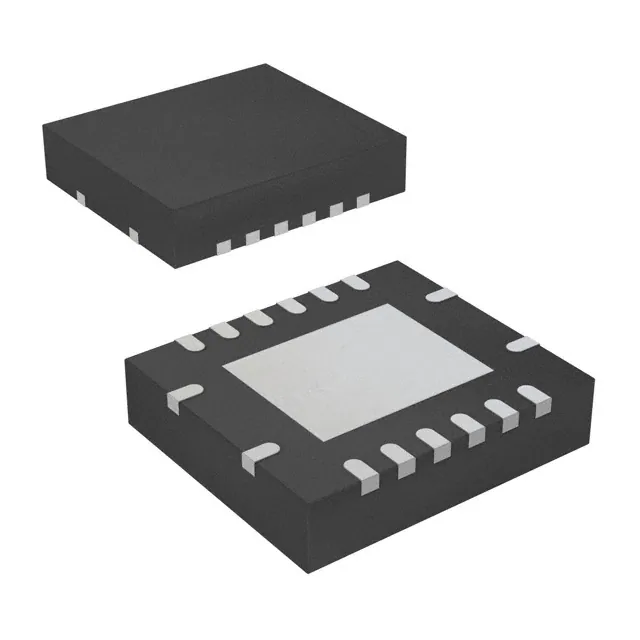
Package: ATSLP-12-4 (1.1 mm × 1.9 mm × 0.65 mm), leadless, thermally enhanced, RoHS-compliant surface-mount package with exposed thermal pad.
| Pin/Terminal | Circuit Role | Design Meaning |
|---|---|---|
| RX1–RX5 | RF Input Ports | Five independent antenna receive paths; DC-free operation enables direct connection to LNA inputs without blocking caps. |
| AI | Antenna Interface | Common RF output node connected to transceiver Rx input; supports SP5T switching topology. |
| VBAT | Main Power Supply | Supplies RF switch core and internal logic; accepts battery-level voltage (2.2–5.5 V) directly. |
| VIO | Digital Interface Supply | Powers MIPI RFFE interface; sets logic thresholds for SCLK/SDATA/SSEL signals. |
| SCLK, SDATA, SSEL1, SSEL2 | MIPI RFFE Control Lines | Support 2-wire serial interface per MIPI RFFE v2.0; SSEL1/SSEL2 enable multi-device addressing. |
| GND | Ground Reference | Primary RF and digital ground; requires low-inductance PCB connection to thermal pad. |
Key Features
| Feature | Design Value |
|---|---|
| Integrated MIPI RFFE Controller | Eliminates external MCU or sequencer; supports USID programming and low-power mode transitions via standard commands. |
| DC-Free RF Ports | Removes requirement for external DC-blocking capacitors unless external DC bias is applied-reducing BOM count and board area. |
| High EMI Robustness | Validated against IEC 61000-4-2 (15 kV air/8 kV contact discharge); maintains functionality in noisy smartphone RF environments. |
| Small Form Factor | 1.1 mm × 1.9 mm footprint fits tight antenna-switch module layouts in modern slim smartphones. |
| On-Chip ESD Protection | Integrated HBM/CDM protection on all pins reduces system-level ESD design effort and improves field reliability. |
Applications
| Smartphone LTE/WCDMA Diversity Reception | Multi-Band Mobile Handset Antenna Switching |
|---|---|
Use Scenario: Dual-SIM/dual-active smartphones requiring simultaneous reception from multiple antennas across LTE Bands 1, 3, 7, 20, and WCDMA Band I/II. IC Role / Device Role / Timing Role: SP5T RF switch selects optimal Rx path based on signal quality metrics reported by baseband processor via MIPI RFFE. Use Value: Enables real-time antenna diversity gain up to 3 dB, improving call drop rate and data throughput in weak-signal urban environments. | Use Scenario: Compact mobile handsets with space-constrained antenna layouts needing dynamic reconfiguration of four external antennas and one internal diversity antenna. IC Role / Device Role / Timing Role: Centralized RF path selector controlled by AP's MIPI RFFE master; supports sub-2 µs path switching latency. Use Value: Reduces need for duplicate LNA chains; lowers total Rx chain noise figure by maintaining shortest possible trace length to selected antenna. |
| Tablet Cellular Modem Module | IoT Cellular Gateway with MIMO Support |
Use Scenario: 10-inch LTE tablet integrating two main antennas and three diversity antennas for improved indoor coverage. IC Role / Device Role / Timing Role: Manages five independent Rx paths feeding separate RF front-end receivers in a multi-Rx-chain architecture. Use Value: Achieves >20 dB isolation between adjacent RX ports, preventing desensitization during concurrent multi-band scanning. | Use Scenario: Industrial IoT gateway supporting LTE Cat-M1/NB-IoT with redundant antenna inputs for mission-critical connectivity. IC Role / Device Role / Timing Role: Provides failover path selection between primary and backup antennas under network-controlled MIPI command. Use Value: Ensures continuous Rx link availability during antenna obstruction or environmental fading events without host firmware intervention. |
Equivalent & Alternatives
The following parts are listed as comparable options for similar SP5T RF switch applications.
| Alternative Part | Technical Difference | Application Difference | Selection Advice |
|---|---|---|---|
| Qorvo QM11020 | Higher insertion loss (0.55 dB @ 2.1 GHz); GaAs process; requires external DC blocking caps on all RF ports. | Targeted for cost-sensitive mid-tier smartphones where ESD robustness is secondary to bill-of-materials cost. | Select when legacy GaAs supply chain is preferred and board space allows for added capacitor footprints. |
| Skyworks SKY16605-362LF | SP4T configuration only; lacks fifth Rx port; higher VBAT min (2.7 V); no integrated MIPI RFFE controller. | Used in simpler dual-antenna architectures where full SP5T capability is unnecessary. | Choose only if design uses exactly four Rx paths and external GPIO-based control suffices. |
Compared with QM11020 and SKY16605-362LF, BGS15MC172E6433XUSA1 delivers superior integration (MIPI RFFE + DC-free ports), lower loss, and smaller footprint-making it optimal for high-density, multi-antenna smartphone platforms demanding minimal external components and fast path reconfiguration.
Availability
BGS15MC172E6433XUSA1 is available at Aetrix Electronics and suitable for LTE/WCDMA smartphone designs, cellular tablet modem modules, and industrial IoT gateways requiring stable component supply, consistent RF performance across temperature, and long-term production support.
Supply support for BGS15MC172E6433XUSA1 includes scheduled delivery planning, volume procurement assistance, BOM continuity management, traceable sourcing, and lifecycle availability coordination for OEM customers, industrial embedded developers, connected-device designers, and electronics production programs.
Manufacturer
Infineon Technologies AG is a German semiconductor manufacturer specializing in power management, automotive, industrial, and RF solutions, with global R&D and manufacturing infrastructure.
The BGS15MA12 product line targets high-performance RF front-end modules for mobile communications, emphasizing integration, ESD resilience, and MIPI-standardized control to simplify antenna diversity implementation in space-constrained devices.
FAQ
What is the maximum allowable DC voltage on the RX1–RX5 ports?
The BGS15MC172E6433XUSA1 specifies zero DC voltage (0 V) on all RF ports per datasheet Table 3. External DC bias requires series blocking capacitors; otherwise, internal MOS structure may be damaged. This constraint ensures safe operation of the DC-free RF switch architecture and preserves harmonic suppression performance.
Does this part require external decoupling capacitors on VBAT?
Yes - a minimum 100 nF ceramic capacitor placed within 1 mm of the VBAT pin is required per datasheet Section 7. This stabilizes the internal charge pump and prevents supply droop during fast RF path transitions, ensuring consistent insertion loss and isolation across operating frequencies.
Can the MIPI RFFE interface operate at 1.2 V VIO?
Yes - the device supports VIO from 1.1 V to 1.95 V, including 1.2 V. At this level, VIH is guaranteed ≥0.84 V and VIL ≤0.36 V, matching standard 1.2 V I/O logic families. No level shifters are needed when interfacing with application processors such as Qualcomm Snapdragon or MediaTek Helio SoCs.
How is thermal performance managed in the ATSLP-12-4 package?
The ATSLP-12-4 package incorporates an exposed thermal pad soldered to a dedicated PCB copper pour. Datasheet Figure 13 recommends ≥8 mm² of 2-oz copper connected via ≥4 thermal vias (0.3 mm diameter) to inner ground planes. This achieves ≤45 °C/W junction-to-board thermal resistance, enabling continuous 27 dBm operation at 85 °C ambient.
BGS15MC172E6433XUSA1 Specifications
- Product attributes
- Attribute value
- Manufacturer:
- Infineon Technologies
- Series:
- *
- Package/Case:
- -
- Packaging:
- Bulk
- Product Status:
- Active
- Type:
- -
- Circuit:
- -
- Independent Circuits:
- -
- Current - Output High, Low:
- -
- Voltage Supply Source:
- -
- Voltage - Supply:
- -
- Operating Temperature:
- -
- Grade:
- -
- Qualification:
- -
- Mounting Type:
- -
- Supplier Device Package:
- -
BGS15MC172E6433XUSA1 FAQ
1.How can I place an order for BGS15MC172E6433XUSA1 through Aetrix?
Please submit a Request for Quotation (RFQ) for BGS15MC172E6433XUSA1 on Aetrix. Our sales agent will provide a competitive quotation and guide you through the order confirmation once you accept the terms.
2.Are the price and stock information for BGS15MC172E6433XUSA1 reliable?
The price and inventory of BGS15MC172E6433XUSA1 are updated periodically and may fluctuate due to market conditions. Stock and pricing data are typically refreshed every 24 hours. Quotation validity for BGS15MC172E6433XUSA1 is usually 5 days.
3.What payment methods are accepted for BGS15MC172E6433XUSA1?
We accept Wire Transfer, PayPal, Credit Card, Western Union, MoneyGram, and Escrow for BGS15MC172E6433XUSA1 transactions.
Note: Certain payment methods may incur a processing fee.
4.How is shipping managed for BGS15MC172E6433XUSA1?
BGS15MC172E6433XUSA1 orders can be shipped via leading logistics carriers, including DHL, UPS, FedEx, TNT, or Registered Mail.
Once your BGS15MC172E6433XUSA1 order is processed, you will receive an email with the shipment details and tracking number.
Note: Tracking information may take up to 24 hours to appear. Express delivery typically takes 3–5 business days.
5.How can I obtain technical support or documentation for BGS15MC172E6433XUSA1?
For technical support, including BGS15MC172E6433XUSA1 datasheets, pinout diagrams, or application guidance, please contact our engineering support team. They can provide detailed documentation and assistance for your BGS15MC172E6433XUSA1 requirements.
6.How does Aetrix verify that BGS15MC172E6433XUSA1 is sourced from the original manufacturer or authorized distributors?
All BGS15MC172E6433XUSA1 products on Aetrix are procured from qualified distributors and authorized channels. Our dedicated quality assurance team conducts strict verification, including traceability checks and, if necessary, third-party testing. This ensures that BGS15MC172E6433XUSA1 meets industry standards.
7.What is the process for return or replacement of BGS15MC172E6433XUSA1?
All BGS15MC172E6433XUSA1 units undergo pre-shipment inspection (PSI). If there is an issue with BGS15MC172E6433XUSA1, returns or replacements are accepted under the following conditions:
1.Quantity discrepancies, incorrect items, or visible external defects (such as breakage or corrosion), acknowledged by Aetrix.
2.The issue is reported within 90 days of delivery.
3.The BGS15MC172E6433XUSA1 part is unused and in its original packaging.
Return procedure for BGS15MC172E6433XUSA1:
1.Submit a request within 90 days.
2.Obtain a Return Material Authorization (RMA) from Aetrix.
BGS15MC172E6433XUSA1 Tags

-
SN74HC138DR
Texas Instruments
-
TC7SB3157CFU,LF(CT
Toshiba Semiconductor and Storage
-
74CBTLV3257PW,118
Nexperia USA Inc.

-
SN74CBTLV3257PWR
Texas Instruments
-
74CBTLV3257GUX
Nexperia USA Inc.
-
74HC154BQ,118
Nexperia USA Inc.

-
P3S0200GMX
NXP USA Inc.

-
SN74CB3Q3245PWR
Texas Instruments
-
SN74CB3Q3257RGYR
Texas Instruments

-
TCA9543APWR
Texas Instruments
-
TCA9546APWR
Texas Instruments

-
SN74HC138N
Texas Instruments
Tech Hub

Operational amplifier guide covering op amp basics, feedback, ideal vs real op amps, common configurations, buffer circuits, offset, bias current, gain-bandwidth, slew rate, rail-to-rail limits and sel…

Jumper cables guide covering safe connection order, red and black clamp placement, final ground connection, cable gauge, length, clamp quality, copper vs CCA cables, jump starter comparison and battery…

LDO regulator guide covering low dropout voltage, power dissipation, thermal design, PSRR, output noise, capacitor stability, adjustable LDO circuits, LDO vs buck converter and datasheet selection chec…

Conditional Access Module guide covering CAM meaning, CI/CI+ interface, smart card authorization, DVB security workflow, TV and set-top box compatibility, internal electronics, ESD protection, connecto…

Guide to electronic component obsolescence covering EOL risk, PCN/PDN notices, last-time buy planning, replacement options, form-fit-function validation, counterfeit risk and BOM lifecycle management.

18650 battery guide covering lithium-ion cell basics, 3.6V/3.7V voltage, 4.2V charging, mAh and Wh capacity, protected cells, chargers, BMS, series-parallel packs, holders, welding and sourcing checks.…

Hall effect sensor guide covering working principle, linear and digital sensors, Arduino circuits, current sensing, speed detection, automotive applications, A3144 examples, signal filtering and datash…

Product Change Notification guide for electronic components, covering PCN meaning, PCN vs PDN/EOL, common change types, risk levels, form-fit-function review, engineering validation, BOM control, LTB/L…

A practical guide to blend door actuators, covering HVAC function, symptoms, location, AC and heater issues, reset and calibration, replacement cost, electrical diagnosis, compatibility checks, and rep…

Engineering guide to Raspberry Pi alternatives, covering chip-level differences, Orange Pi, ROCK, Jetson, Banana Pi, NanoPi, Compute Module, Pico, GPIO, camera, HAT compatibility, and replacement risks…


