
 My Inquiry
 My Account


NXP Semiconductors BGS67A,112
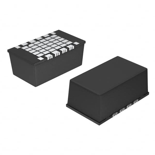
- Part No.:
- BGS67A,112
- Manufacturer:
- NXP Semiconductors
- Category:
- Video Amps and Modules
- Package:
- SOT-567A
- Datasheet:
-
 BGS67A,112.pdf
- Description:
- IC AMP CATV DMAN8
- Quantity:
- Payment:

- Shipping:

Inventory:3,766
Please send an inquiry. Send us your inquiry, and we will respond immediately.
Product details
Overview
BGS67A,112 from NXP Semiconductors (formerly Philips Semiconductors) is a hybrid high dynamic range reverse amplifier module designed for CATV return-path amplification. It delivers 25.5 dB power gain at 10 MHz, operates from a 12 V supply with 75–95 mA total current draw, and supports 5–65 MHz bandwidth with ±0.2 dB flatness and 3.5 dB noise figure at 65 MHz.
For engineers reviewing the BGS67A,112 datasheet, BGS67A,112 pinout, BGS67A,112 application, or BGS67A,112 equivalent, key selection criteria include its SOT567A leadless package, dual +VB and common terminals, rugged silicon nitride passivation, and verified CTB (−64 dB) and Xmod (−54 dB) performance in multi-channel CATV systems.
Technical Context
The BGS67A,112 functions as a broadband reverse-path amplifier in two-way cable networks, optimized for 5–65 MHz upstream signal conditioning. Its hybrid construction integrates active and passive elements to achieve excellent linearity (CTB ≤ −64 dB, Xmod ≤ −54 dB) and low noise (NF = 3.5 dB), while maintaining input/output return loss ≥20 dB across the band.
It employs gold metallization and silicon nitride passivation for reliability under thermal cycling and humidity stress. The module withstands supply transients up to 30 V despite nominal 12 V operation, and requires ESD-handling precautions per IEC 61340-5-1 due to sensitivity to electrostatic discharge.
Key Specifications
| Parameter | Value and Actual Design Meaning |
|---|---|
| Power Gain | 25.5 dB typical at 10 MHz - ensures sufficient upstream signal boost without cascaded distortion |
| Bandwidth | 5 MHz to 65 MHz - covers full DOCSIS-compliant upstream spectrum |
| Noise Figure | 3.5 dB at 65 MHz - preserves upstream SNR in multi-node return-path architectures |
| Composite Triple Beat | −64 dB - meets stringent CATV system linearity requirements for 4-channel flat input |
| Input Return Loss | ≥20 dB - minimizes reflections and impedance mismatch in 75 Ω coaxial distribution |
| Supply Voltage Range | 12 V nominal, 30 V transient tolerant - enables robust operation during power rail disturbances |
| Total Current Draw | 75–95 mA at 12 V - defines thermal load and power supply sizing for amplifier stage design |
Pinout & Package
Package: SOT567A - leadless surface-mounted, plastic cap, 8-termination, 7.1–7.6 mm × 2.35–2.55 mm footprint, with exposed thermal pad (Z6/Z7 dimensions).
| Pin/Terminal | Circuit Role | Design Meaning |
|---|---|---|
| 1 | RF Input | 75 Ω matched input port for upstream CATV signals; s11 ≥20 dB across 5–65 MHz |
| 2 | Common (Ground) | DC and RF ground reference; electrically tied to thermal pad and chassis ground |
| 3 | Provision | Unused terminal; no internal connection - must be left floating or grounded per layout guidelines |
| 4 | +VB (Supply) | Primary 12 V DC supply input; decoupling required within 5 mm of pin |
| 5 | RF Output | 75 Ω matched output driving downstream amplifier or splitter; s22 ≥20 dB |
| 6 | Provision | Unused terminal; no internal connection - must be left floating or grounded per layout guidelines |
| 7 | Common (Ground) | Secondary ground path; enhances thermal dissipation and RF stability |
| 8 | +VB (Supply) | Secondary 12 V DC supply input; used with Pin 4 for balanced supply routing and reduced IR drop |
Key Features
| Feature | Design Value |
|---|---|
| Hybrid High Dynamic Range Architecture | Combines GaAs FET and passive matching for simultaneous low NF (3.5 dB) and high linearity (CTB −64 dB) |
| Silicon Nitride Passivation | Protects die surface against moisture ingress and ion migration, enabling >10-year field reliability in humid outdoor enclosures |
| Gold Metallization | Ensures stable bond wire integrity and low-contact-resistance interconnects over thermal cycling (−20 °C to +100 °C mounting base) |
| Rugged Construction | Withstands 30 V supply transients and mechanical shock per MIL-STD-883H Method 2002.3, suitable for headend and node deployment |
Applications
| Reverse Path Amplifier in HFC Nodes | Upstream Signal Conditioning in Cable Modem Termination Systems |
|---|---|
Use Scenario: Installed in fiber-deep hybrid fiber-coax (HFC) node cabinets to amplify upstream signals from multiple subscriber drops before optical conversion. IC Role / Device Role / Timing Role: Reverse-path RF amplifier providing fixed 25.5 dB gain with minimal added noise and distortion across 5–65 MHz. Use Value: Enables reliable DOCSIS 3.1 upstream operation by maintaining CTB ≤ −64 dB and NF ≤ 3.5 dB under full channel loading. | Use Scenario: Embedded in CMTS line cards to condition return-path signals prior to ADC sampling and digital processing. IC Role / Device Role / Timing Role: Analog front-end gain block ensuring adequate signal level and spectral purity for digitization at 125 MSPS. Use Value: Delivers ±0.2 dB gain flatness and ≥20 dB return loss, reducing equalizer complexity and improving upstream BER. |
| Two-Way CATV Distribution Hub | Return-Path Monitoring and Test Equipment |
Use Scenario: Used in headend distribution hubs to combine and amplify upstream traffic from multiple trunk lines before retransmission. IC Role / Device Role / Timing Role: High-linearity broadband amplifier supporting multi-port aggregation without intermodulation degradation. Use Value: Achieves −54 dB Xmod and −64 dB CTB at 50 dBmV output, preventing cross-talk between aggregated upstream channels. | Use Scenario: Integrated into portable field test sets for real-time measurement of upstream signal quality in live plant environments. IC Role / Device Role / Timing Role: Stable, calibrated gain stage enabling accurate dBmV-level signal injection and response analysis. Use Value: Maintains consistent 25.5 dB gain and <0.6 dB slope across 5–65 MHz, eliminating calibration drift during on-site diagnostics. |
Equivalent & Alternatives
The following parts are listed as comparable options for similar reverse-path amplifier applications.
| Alternative Part | Technical Difference | Application Difference | Selection Advice |
|---|---|---|---|
| MAX2472EUT+T | 50 Ω system, 20–450 MHz bandwidth, 15.5 dB gain, higher NF (4.5 dB), SO-8 package | Designed for general-purpose RF gain blocks, not optimized for 75 Ω CATV return-path linearity or CTB | Use only where 75 Ω impedance matching and CATV-specific distortion specs are not required |
| QPL9057TR13 | 75 Ω, 5–65 MHz, 23 dB gain, −62 dB CTB, 4.2 dB NF, 3×3 mm QFN | Lower gain and higher noise than BGS67A,112; lacks dual +VB pins and ruggedized passivation | Acceptable for cost-sensitive, lower-performance return-path stages where thermal robustness is secondary |
Compared with MAX2472EUT+T and QPL9057TR13, the BGS67A,112 provides superior CATV-specific performance: 25.5 dB gain, −64 dB CTB, 3.5 dB NF, and dual-supply-pin architecture in a thermally enhanced SOT567A package - making it uniquely suited for mission-critical upstream amplification in outdoor nodes and headends.
Availability
BGS67A,112 is available at Aetrix Electronics and suitable for CATV node upgrades, cable modem termination systems, and two-way distribution hub designs requiring stable component supply, long-lifecycle support, and proven field reliability in harsh environmental conditions.
Supply support for BGS67A,112 includes scheduled delivery planning, volume procurement assistance, BOM continuity management, traceable sourcing, and lifecycle availability coordination for OEM customers, industrial embedded developers, connected-device designers, and electronics production programs.
Manufacturer
NXP Semiconductors is a global semiconductor leader focused on secure connectivity solutions for automotive, industrial, and communications markets, with roots in Philips' pioneering analog and RF technology.
The BGS67A,112 belongs to NXP's legacy CATV amplifier portfolio, engineered specifically for high-reliability reverse-path signal conditioning in hybrid fiber-coax infrastructure - emphasizing linearity, noise control, and rugged packaging for outdoor deployment.
FAQ
What is the operating supply voltage range for the BGS67A,112?
The BGS67A,112 operates nominally at 12 V DC but is rated to withstand supply transients up to 30 V without damage. Total current consumption ranges from 75 mA to 95 mA at 12 V, and the device requires proper decoupling on both +VB pins (Pins 4 and 8) to ensure stable RF performance and thermal management.
Does the BGS67A,112 require external biasing or tuning components?
No, the BGS67A,112 is a fully self-contained hybrid amplifier module with internal biasing and impedance matching. It requires only DC blocking capacitors (typically 100 pF) on input and output, plus 10 µF/100 nF parallel decoupling on each +VB pin. No external inductors, resistors, or trimmers are needed for standard 75 Ω CATV operation.
How does the BGS67A,112 handle thermal management in enclosed node housings?
The BGS67A,112 uses a thermally enhanced SOT567A package with an exposed metal pad (Z6/Z7) that must be soldered to a dedicated copper thermal land on the PCB. Mounting base temperature is rated from −20 °C to +100 °C, and proper thermal vias beneath the pad reduce junction-to-ambient resistance, enabling reliable operation in sealed outdoor enclosures without forced airflow.
Is the BGS67A,112 compatible with DOCSIS 4.0 upstream channel bonding?
The BGS67A,112 supports the 5–65 MHz frequency band used in DOCSIS 3.0 and earlier upstream profiles. While it does not extend to the extended upstream spectrum (up to 204 MHz) required for DOCSIS 4.0 channel bonding, its −64 dB CTB and ±0.2 dB flatness remain fully compliant for legacy and current-generation upstream deployments in existing HFC plants.
What ESD precautions are required when handling the BGS67A,112?
The BGS67A,112 is highly sensitive to electrostatic discharge (ESD), per IEC 61340-5-1 Class 1A (≤250 V). Handlers must use grounded wrist straps, ESD-safe work surfaces, conductive foam storage, and ionized air environments. PCB assembly requires ESD-safe soldering irons and automated placement equipment with static-dissipative nozzles to prevent latent damage to the hybrid die.
BGS67A,112 Specifications
- Product attributes
- Attribute value
- Manufacturer:
- NXP Semiconductors
- Package/Case:
- SOT-567A
- Series:
- -
- Packaging:
- Bulk
- Product Status:
- Obsolete
- Applications:
- CATV
- Output Type:
- -
- Number of Circuits:
- 1
- -3db Bandwidth:
- -
- Slew Rate:
- -
- Current - Supply:
- 95 mA
- Current - Output / Channel:
- -
- Voltage - Supply, Single/Dual (±):
- -
- Mounting Type:
- Surface Mount
- Grade:
- -
- Qualification:
- -
- Supplier Device Package:
- DMAN8
BGS67A,112 FAQ
1.How can I place an order for BGS67A,112 through Aetrix?
Please submit a Request for Quotation (RFQ) for BGS67A,112 on Aetrix. Our sales agent will provide a competitive quotation and guide you through the order confirmation once you accept the terms.
2.Are the price and stock information for BGS67A,112 reliable?
The price and inventory of BGS67A,112 are updated periodically and may fluctuate due to market conditions. Stock and pricing data are typically refreshed every 24 hours. Quotation validity for BGS67A,112 is usually 5 days.
3.What payment methods are accepted for BGS67A,112?
We accept Wire Transfer, PayPal, Credit Card, Western Union, MoneyGram, and Escrow for BGS67A,112 transactions.
Note: Certain payment methods may incur a processing fee.
4.How is shipping managed for BGS67A,112?
BGS67A,112 orders can be shipped via leading logistics carriers, including DHL, UPS, FedEx, TNT, or Registered Mail.
Once your BGS67A,112 order is processed, you will receive an email with the shipment details and tracking number.
Note: Tracking information may take up to 24 hours to appear. Express delivery typically takes 3–5 business days.
5.How can I obtain technical support or documentation for BGS67A,112?
For technical support, including BGS67A,112 datasheets, pinout diagrams, or application guidance, please contact our engineering support team. They can provide detailed documentation and assistance for your BGS67A,112 requirements.
6.How does Aetrix verify that BGS67A,112 is sourced from the original manufacturer or authorized distributors?
All BGS67A,112 products on Aetrix are procured from qualified distributors and authorized channels. Our dedicated quality assurance team conducts strict verification, including traceability checks and, if necessary, third-party testing. This ensures that BGS67A,112 meets industry standards.
7.What is the process for return or replacement of BGS67A,112?
All BGS67A,112 units undergo pre-shipment inspection (PSI). If there is an issue with BGS67A,112, returns or replacements are accepted under the following conditions:
1.Quantity discrepancies, incorrect items, or visible external defects (such as breakage or corrosion), acknowledged by Aetrix.
2.The issue is reported within 90 days of delivery.
3.The BGS67A,112 part is unused and in its original packaging.
Return procedure for BGS67A,112:
1.Submit a request within 90 days.
2.Obtain a Return Material Authorization (RMA) from Aetrix.
BGS67A,112 Tags

-
LT6552CS8#PBF
Analog Devices Inc.
-
LT6205IS5#TRPBF
Analog Devices Inc.
-
LT6206IMS8#TRPBF
Analog Devices Inc.
-
LT6552CDD#PBF
Analog Devices Inc.
-
LT6552IS8#PBF
Analog Devices Inc.
-
LT1252CS8#PBF
Analog Devices Inc.
-
AD818ARZ-REEL7
Analog Devices Inc.

-
MAX4310EUA+
Analog Devices Inc./Maxim Integrated
-
AD829ARZ
Analog Devices Inc.
-
AD810ARZ
Analog Devices Inc.

-
MAX4310ESA+
Analog Devices Inc./Maxim Integrated
-
MAX4313ESA+
Analog Devices Inc./Maxim Integrated
Tech Hub

A practical engineering guide to 3.3V and 5V logic compatibility, input thresholds, resistor dividers, translator ICs, MOSFET level shifting, I2C pull-ups, timing limits and power-sequencing risks.

The 74HC595 uses push-pull logic outputs, while the TPIC6B595 uses 50 V open-drain DMOS sinks for higher-power loads. This guide compares timing, current limits, 3.3 V interfacing, load wiring, thermal…

The 74HC595 converts serial data into eight stable parallel outputs. This guide covers pin functions, shift and storage timing, OE and MR behavior, drive-current limits, cascading, voltage compatibilit…

A technical comparison of level-sensitive latches and edge-triggered flip-flops, covering timing windows, setup and hold limits, master–slave operation, time borrowing, race-through, HDL inference and…

A D latch stores one bit while Enable controls when data can pass. This reference covers gate-level operation, truth tables, transparency, setup and hold timing, LE versus OE, common ICs and practical …

An SR latch stores one bit through cross-coupled feedback. This engineering reference covers NOR and NAND implementations, truth tables, forbidden-state recovery, gated operation, switch debouncing, fa…

Latch circuits retain one bit through feedback. This technical reference covers SR and D latches, truth tables, transparency, timing limits, latch-versus-flip-flop behavior, applications and common log…

An engineering guide to LED driver operation, constant-current and constant-voltage outputs, linear and switching topologies, dimming, IC selection, calculations, replacement compatibility, and fault c…

Operational amplifier guide covering op amp basics, feedback, ideal vs real op amps, common configurations, buffer circuits, offset, bias current, gain-bandwidth, slew rate, rail-to-rail limits and sel…

Jumper cables guide covering safe connection order, red and black clamp placement, final ground connection, cable gauge, length, clamp quality, copper vs CCA cables, jump starter comparison and battery…


