
 My Inquiry
 My Account


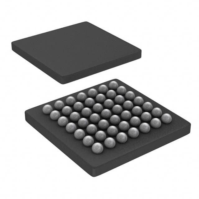
Texas Instruments BQ24161YFFR
- Part No.:
- BQ24161YFFR
- Manufacturer:
- Texas Instruments
- Category:
- Battery Chargers
- Package:
- 49-UFBGA, DSBGA
- Datasheet:
-
 BQ24161YFFR.pdf
- Description:
- IC BATT CHG LI-ION 1CELL 49DSBGA
- Quantity:
- Payment:

- Shipping:

Inventory:2,978
Please send an inquiry. Send us your inquiry, and we will respond immediately.
Product details
Overview
BQ24161YFFR from Texas Instruments is a 2.5-A dual-input switched-mode Li-ion battery charger with integrated power path management and I²C interface, designed for portable systems requiring simultaneous system power and battery charging. It supports USB (up to 1.5 A) and IN (up to 2.5 A at 10.5 V) inputs, delivers 1% battery voltage regulation accuracy, and enables instant system startup from a deeply discharged or absent battery.
For engineers reviewing the BQ24161YFFR datasheet, BQ24161YFFR pinout, BQ24161YFFR application, or BQ24161YFFR equivalent, this device is selected for space-constrained, high-capacity battery applications where input source selection, JEITA-compliant NTC monitoring, and programmable charge parameters via I²C are critical design requirements.
Technical Context
The BQ24161YFFR implements a synchronous buck converter topology with dual independent input paths (USB and IN), each featuring dedicated overvoltage protection (6.5 V for USB, 10.5 V for IN) and programmable current limits via I²C. Its power path architecture separates system power (SYS) from battery charging (BAT), allowing the system to operate directly from input while charging the battery concurrently.
It integrates internal MOSFETs-including top-side reverse-blocking FETs (95 mΩ USB path, 45 mΩ IN path), switching FETs (100–110 mΩ), and bottom-side sync FET (65–115 mΩ)-and supports JEITA-compliant thermal regulation using the TS pin with four threshold levels (VHOT, VWARM, VCOOL, VCOLD) referenced to DRV voltage.
Key Specifications
| Parameter | Value and Actual Design Meaning |
|---|---|
| Charge Current | Programmable up to 2.5 A; enables fast charging of high-capacity single-cell Li-ion batteries in portable devices. |
| Battery Regulation Accuracy | ±1%; ensures precise 3.5–4.44 V charge voltage control, critical for battery longevity and safety compliance. |
| Input Voltage Ranges | USB: 4.2–6 V (OVP = 6.5 V); IN: 4.2–10.5 V (OVP = 10.5 V); supports dual-source flexibility without external switching. |
| Power Path Management | Enables SYS output regulation (3.7 V typical) independent of battery state; allows system operation with dead/absent battery. |
| I²C Interface | Full register access for real-time configuration of charge parameters, fault masks, timers, and NTC thresholds. |
| NTC Monitoring | JEITA-compatible 4-threshold detection (VHOT/VWARM/VCOOL/VCOLD) using TS pin; supports safe charging across temperature extremes. |
| Package | 2.8 mm × 2.8 mm 49-ball DSBGA (YFF); ultra-compact footprint ideal for thin handheld and wearable designs. |
Pinout & Package
Package: 49-ball DSBGA (YFF), 2.8 mm × 2.8 mm, 0.4 mm pitch, thermal pad connected to PGND.
| Pin/Terminal | Circuit Role | Design Meaning |
|---|---|---|
| BAT | Battery terminal | Connects directly to Li-ion cell anode; bypassed with ≥1 µF capacitor for stability during charge/discharge transients. |
| SYS | System power rail sense | Monitors and regulates system output voltage; connects to bulk capacitors at system load to maintain stable 3.7 V under dynamic loads. |
| USB / IN | Dual input power sources | USB accepts 4.2–6 V (1.5 A max); IN accepts 4.2–10.5 V (2.5 A max); fully isolated and selectable via I²C. |
| PSEL | USB source detection control | Logic input selecting USB current limit: high = 100 mA (BQ24161), low = 1.5 A; eliminates need for D+/D− detection circuitry. |
| TS | NTC thermistor interface | Analog input for resistor-divider network; enables JEITA-compliant charging by detecting battery temperature at four thresholds. |
| SCL / SDA | I²C communication bus | Standard two-wire interface for configuring charge profiles, reading faults, and enabling/disabling features in real time. |
| STAT / INT | Status interrupt outputs | Open-drain signals indicating charge status (STAT) and faults (INT); support host processor polling or interrupt-driven response. |
Key Features
| Feature | Design Value |
|---|---|
| Instant System Startup | Delivers regulated SYS voltage even with 0 V battery or no battery installed-eliminates boot failure in deeply discharged devices. |
| Dual-Input Source Selection | Hardware- and I²C-selectable USB/IN paths with independent OVP and current limiting-enables flexible power architecture without external muxing. |
| JEITA-Compatible NTC Monitoring | Four programmable thermal thresholds (VHOT/VWARM/VCOOL/VCOLD) on TS pin-ensures safe charging across -10°C to +60°C ambient ranges. |
| Integrated Power Path FETs | Internal top-side reverse-blocking FETs (95 mΩ USB, 45 mΩ IN) and synchronous buck switches-reduces BOM count and PCB area vs. discrete solutions. |
| Programmable Safety Timers | Configurable charge timeout, pre-charge timer, and termination delay via I²C registers-supports custom battery chemistries and aging compensation. |
Applications
| Smartphone Power Management | Wireless Headphone Charging |
|---|---|
|
Use Scenario: Compact smartphone with dual-input charging (USB-C and wireless receiver) and requirement for uninterrupted system operation during battery charging. IC Role / Device Role: Primary battery charger and power path manager that routes input power to SYS while independently charging the 3.8 V, 4000 mAh Li-ion cell. Use Value: Enables zero-downtime user experience-system powers on instantly even after full discharge, and battery charges at 2.5 A without throttling CPU performance. |
Use Scenario: True wireless stereo (TWS) earbud case with USB input and embedded Qi receiver, needing compact, thermally robust charging. IC Role / Device Role: Dual-input Li-ion charger managing both wired and wireless power sources, with JEITA-compliant thermal cutoff for small-form-factor battery packs. Use Value: Prevents overheating during rapid charging in confined space; TS pin thresholds ensure safe 0.5 A–1.2 A charge rates across ambient temperatures from 0°C to 45°C. |
| Portable Medical Monitor | Rugged Handheld Scanner |
|
Use Scenario: Battery-powered clinical monitor requiring FDA-grade reliability, cold-weather operation, and hot-swap battery capability. IC Role / Device Role: Safety-critical charger with VMINSYS regulation (3.5 V), battery short-circuit protection (VBATSHRT = 2.0 V), and thermal shutdown (165°C). Use Value: Guarantees continuous display and sensor operation down to –20°C via VWARM/VCOOL thresholds; BATGD pin confirms battery presence before enabling charge. |
Use Scenario: Industrial barcode scanner used in warehouses with frequent AC adapter and USB cable swaps, subject to ESD and voltage transients. IC Role / Device Role: Robust dual-input charger with 2 kV HBM ESD rating, 10.5 V IN OVP, and programmable input current limits to prevent adapter overload. Use Value: Eliminates field failures from misconnected adapters or damaged cables; PSEL pin simplifies source detection without D+/D− analog circuitry. |
Equivalent & Alternatives
The following parts are listed as comparable options for similar dual-input Li-ion charger applications.
| Alternative Part | Technical Difference | Application Difference | Selection Advice |
|---|---|---|---|
| BQ24163YFFT | Same YFF package; supports lower VMINSYS (3.2 V) and VBATSHRT (1.9 V), but lacks JEITA NTC support-uses standard 2-threshold TS monitoring. | Preferred for cost-sensitive industrial tools where extended low-temperature charging is not required. | Select BQ24163YFFT when JEITA compliance is unnecessary and minimum system voltage tolerance is more critical than thermal granularity. |
| BQ24161BRGRT | VQFN-24 (4 mm × 4 mm) package; identical electrical specs and JEITA support, but larger footprint and higher θJA (32.6°C/W vs. 49.8°C/W for YFF). | Better suited for thermally relaxed designs with available PCB area and need for rework-friendly QFN assembly. | Choose BQ24161BRGRT if board layout permits larger package and thermal management relies on copper pour rather than minimal footprint. |
Compared with BQ24161YFFR, BQ24163YFFT trades JEITA thermal precision for wider battery short-circuit tolerance, while BQ24161BRGRT offers identical functionality in a rework-friendly QFN-but with 37% higher junction-to-ambient thermal resistance, demanding more aggressive PCB thermal design.
Availability
BQ24161YFFR is available at Aetrix Electronics and suitable for smartphone power management, wireless audio charging, portable medical monitors, and rugged handheld scanners requiring stable component supply across high-volume production cycles.
Supply support for BQ24161YFFR includes scheduled delivery planning, volume procurement assistance, BOM continuity management, traceable sourcing, and lifecycle availability coordination for OEM customers, industrial embedded developers, connected-device designers, and electronics production programs.
Manufacturer
Texas Instruments is a global semiconductor leader specializing in analog, embedded processing, and power management ICs, with decades of expertise in battery charging and power path architectures.
The BQ24161YFFR belongs to TI's BQ2416xx family of highly integrated Li-ion chargers, engineered specifically for space-constrained portable electronics that demand dual-input flexibility, JEITA thermal safety, and seamless system-battery power arbitration.
FAQ
What input voltage ranges does the BQ24161YFFR support?
The BQ24161YFFR supports two independent input rails: USB input from 4.2 V to 6.0 V (with 6.5 V overvoltage protection), and IN input from 4.2 V to 10.5 V (with 10.5 V overvoltage protection). Both inputs are fully isolated and selectable via I²C or hardware (PSEL for USB). This dual-input capability allows the BQ24161YFFR to serve as a universal charger across USB ports, AC adapters, and wireless power receivers without external switching components.
How does the BQ24161YFFR enable instant system startup with a dead battery?
The BQ24161YFFR implements true power path management: its internal buck converter regulates the SYS output voltage (typically 3.7 V) directly from the input source (USB or IN), independent of battery voltage. Even when the battery is at 0 V or removed, the BQ24161YFFR delivers stable system power-allowing microcontrollers and displays to boot immediately. Only after system stabilization does it begin trickle-charging the battery, ensuring zero downtime in consumer and medical portable devices using the BQ24161YFFR.
Does the BQ24161YFFR support JEITA-compliant battery charging?
Yes, the BQ24161YFFR supports JEITA-compliant charging through its TS pin, which monitors an NTC thermistor via a resistor divider referenced to the DRV rail. It implements four precise thresholds-VHOT (30% DRV), VWARM (38.3% DRV), VCOOL (56.5% DRV), and VCOLD (60% DRV)-each with hysteresis, enabling full JEITA profile enforcement (e.g., reduce charge current above 45°C or below 0°C). This capability is confirmed in the device comparison table and electrical characteristics section of the BQ24161YFFR datasheet.
What is the function of the PSEL pin on the BQ24161YFFR?
The PSEL pin on the BQ24161YFFR is a digital input that selects the USB input current limit at startup: logic high configures 100 mA mode (USB100), and logic low configures 1.5 A mode (USB150). Unlike the BQ24160's D+/D− detection, PSEL eliminates analog sensing circuitry and provides deterministic, noise-immune source identification. It has no effect on the IN input and must be actively driven-floating is prohibited. This feature simplifies design and improves reliability in USB-C and proprietary adapter applications using the BQ24161YFFR.
What package type and size is the BQ24161YFFR supplied in?
The BQ24161YFFR is supplied in a 49-ball DSBGA (Die Size Ball Grid Array) package, designated YFF, with nominal dimensions of 2.8 mm × 2.8 mm and 0.4 mm ball pitch. The thermal pad underneath is electrically connected to PGND and must be soldered to a dedicated PCB ground plane for thermal and electrical integrity. This ultra-compact package enables use in thin-profile portable devices where board space is constrained-such as TWS earbuds, smartwatches, and compact medical sensors-making the BQ24161YFFR ideal for next-generation wearables.
BQ24161YFFR Specifications
- Product attributes
- Attribute value
- Manufacturer:
- Texas Instruments
- Series:
- -
- Package/Case:
- 49-UFBGA, DSBGA
- Packaging:
- Tape & Reel (TR)
- Product Status:
- Active
- Battery Chemistry:
- Lithium Ion/Polymer
- Number of Cells:
- 1
- Current - Charging:
- Constant - Programmable
- Programmable Features:
- -
- Fault Protection:
- Over Temperature, Over Voltage
- Charge Current - Max:
- 2.5A
- Battery Pack Voltage:
- 3.7V
- Voltage - Supply (Max):
- 10V
- Interface:
- I2C
- Operating Temperature:
- -40°C ~ 85°C (TA)
- Grade:
- -
- Qualification:
- -
- Mounting Type:
- Surface Mount
- Supplier Device Package:
- 49-DSBGA (2.8x2.8)
BQ24161YFFR FAQ
1.How can I place an order for BQ24161YFFR through Aetrix?
Please submit a Request for Quotation (RFQ) for BQ24161YFFR on Aetrix. Our sales agent will provide a competitive quotation and guide you through the order confirmation once you accept the terms.
2.Are the price and stock information for BQ24161YFFR reliable?
The price and inventory of BQ24161YFFR are updated periodically and may fluctuate due to market conditions. Stock and pricing data are typically refreshed every 24 hours. Quotation validity for BQ24161YFFR is usually 5 days.
3.What payment methods are accepted for BQ24161YFFR?
We accept Wire Transfer, PayPal, Credit Card, Western Union, MoneyGram, and Escrow for BQ24161YFFR transactions.
Note: Certain payment methods may incur a processing fee.
4.How is shipping managed for BQ24161YFFR?
BQ24161YFFR orders can be shipped via leading logistics carriers, including DHL, UPS, FedEx, TNT, or Registered Mail.
Once your BQ24161YFFR order is processed, you will receive an email with the shipment details and tracking number.
Note: Tracking information may take up to 24 hours to appear. Express delivery typically takes 3–5 business days.
5.How can I obtain technical support or documentation for BQ24161YFFR?
For technical support, including BQ24161YFFR datasheets, pinout diagrams, or application guidance, please contact our engineering support team. They can provide detailed documentation and assistance for your BQ24161YFFR requirements.
6.How does Aetrix verify that BQ24161YFFR is sourced from the original manufacturer or authorized distributors?
All BQ24161YFFR products on Aetrix are procured from qualified distributors and authorized channels. Our dedicated quality assurance team conducts strict verification, including traceability checks and, if necessary, third-party testing. This ensures that BQ24161YFFR meets industry standards.
7.What is the process for return or replacement of BQ24161YFFR?
All BQ24161YFFR units undergo pre-shipment inspection (PSI). If there is an issue with BQ24161YFFR, returns or replacements are accepted under the following conditions:
1.Quantity discrepancies, incorrect items, or visible external defects (such as breakage or corrosion), acknowledged by Aetrix.
2.The issue is reported within 90 days of delivery.
3.The BQ24161YFFR part is unused and in its original packaging.
Return procedure for BQ24161YFFR:
1.Submit a request within 90 days.
2.Obtain a Return Material Authorization (RMA) from Aetrix.
BQ24161YFFR Tags

-
BQ21040DBVR
Texas Instruments

-
MCP73812T-420I/OT
Microchip Technology
-
MCP73831T-2ACI/OT
Microchip Technology
-
MCP73832T-2ACI/OT
Microchip Technology
-
MCP73831T-2DCI/OT
Microchip Technology
-
MCP73832T-2DCI/OT
Microchip Technology
-
MCP73831T-2ATI/OT
Microchip Technology
-
MCP73832T-2ATI/OT
Microchip Technology
-
MCP73831T-5ACI/OT
Microchip Technology

-
MCP73832T-2ACI/MC
Microchip Technology
-
MCP73831T-2ACI/MC
Microchip Technology
-
MCP73831T-2ATI/MC
Microchip Technology
Tech Hub

A practical engineering guide to 3.3V and 5V logic compatibility, input thresholds, resistor dividers, translator ICs, MOSFET level shifting, I2C pull-ups, timing limits and power-sequencing risks.

The 74HC595 uses push-pull logic outputs, while the TPIC6B595 uses 50 V open-drain DMOS sinks for higher-power loads. This guide compares timing, current limits, 3.3 V interfacing, load wiring, thermal…

The 74HC595 converts serial data into eight stable parallel outputs. This guide covers pin functions, shift and storage timing, OE and MR behavior, drive-current limits, cascading, voltage compatibilit…

A technical comparison of level-sensitive latches and edge-triggered flip-flops, covering timing windows, setup and hold limits, master–slave operation, time borrowing, race-through, HDL inference and…

A D latch stores one bit while Enable controls when data can pass. This reference covers gate-level operation, truth tables, transparency, setup and hold timing, LE versus OE, common ICs and practical …

An SR latch stores one bit through cross-coupled feedback. This engineering reference covers NOR and NAND implementations, truth tables, forbidden-state recovery, gated operation, switch debouncing, fa…

Latch circuits retain one bit through feedback. This technical reference covers SR and D latches, truth tables, transparency, timing limits, latch-versus-flip-flop behavior, applications and common log…

An engineering guide to LED driver operation, constant-current and constant-voltage outputs, linear and switching topologies, dimming, IC selection, calculations, replacement compatibility, and fault c…

Operational amplifier guide covering op amp basics, feedback, ideal vs real op amps, common configurations, buffer circuits, offset, bias current, gain-bandwidth, slew rate, rail-to-rail limits and sel…

Jumper cables guide covering safe connection order, red and black clamp placement, final ground connection, cable gauge, length, clamp quality, copper vs CCA cables, jump starter comparison and battery…


