
 My Inquiry
 My Account


Texas Instruments BQ4014YMB-85
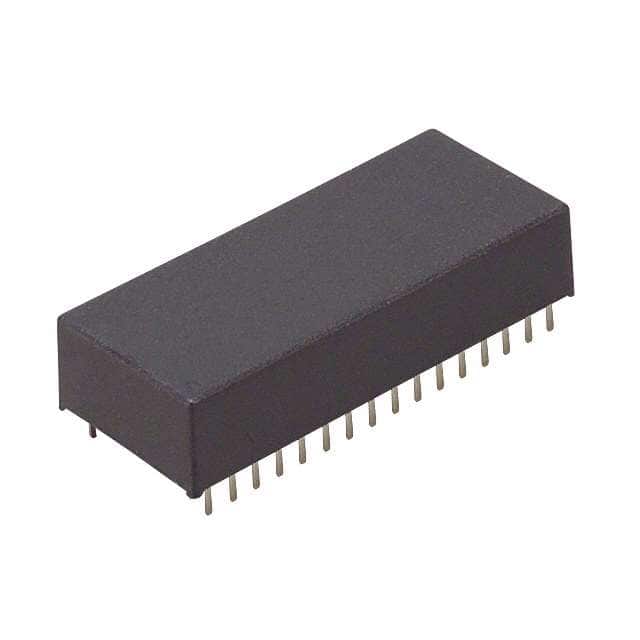
- Part No.:
- BQ4014YMB-85
- Manufacturer:
- Texas Instruments
- Category:
- Memory
- Package:
- 32-DIP Module (0.61", 15.49mm)
- Datasheet:
-
 BQ4014YMB-85.pdf
- Description:
- IC NVSRAM 2MBIT PAR 32DIP MODULE
- Quantity:
- Payment:

- Shipping:

Inventory:2,174
Please send an inquiry. Send us your inquiry, and we will respond immediately.
Product details
Overview
BQ4014YMB-85 from Texas Instruments is a 256K × 8 nonvolatile static RAM (NVSRAM) with integrated lithium backup, 85 ns access time, -10% supply tolerance, and industry-standard 32-pin DIP module packaging. It functions as a standard SRAM during normal operation and automatically preserves data during power loss via internal battery switchover at 3 V, supporting mission-critical data logging in industrial controllers.
For engineers reviewing the BQ4014YMB-85 datasheet, BQ4014YMB-85 pinout, BQ4014YMB-85 application, or BQ4014YMB-85 equivalent, key selection criteria include VPFD threshold (4.37 V), tCER recovery time (120 ms max), 10-year data retention, and compatibility with conventional 2 Mb SRAM timing and bus protocols.
Technical Context
The BQ4014YMB-85 integrates CMOS SRAM, lithium coin cell, and analog power-fail detection circuitry in a single 32-pin MB module. Its control logic monitors VCC continuously, triggering write-protection when voltage drops below VPFD = 4.37 V (typical) and switching to internal backup at VSO = 3 V.
During power-up, it enforces a 120 ms chip-enable recovery window (tCER) before allowing writes, ensuring processor stabilization. The device requires no external components and maintains full SRAM read/write functionality - including unlimited write cycles - while delivering nonvolatility without EEPROM-style latency or endurance limits.
Key Specifications
| Parameter | Value and Actual Design Meaning |
|---|---|
| Memory Organization | 262,144 words × 8 bits (2,097,152-bit total) |
| Access Time | 85 ns - defines minimum cycle time for reliable read/write under worst-case VCC and temperature |
| Power-Fail Threshold (VPFD) | 4.37 V typical - triggers automatic write-protection and backup activation in 10% tolerance systems |
| Data Retention | 10 years without VCC - enabled by isolated lithium cells with ≤0.5% annual self-discharge pre-first-power |
| Supply Voltage Range | 4.75 V to 5.5 V - supports stable operation across full commercial temperature range (0°C to +70°C) |
| Standby Current (ISB2) | 2.5–5 mA - measured with CE ≥ VCC − 0.2 V and inputs biased near rail, critical for low-power hold modes |
| Write-Protect Delay (tWPT) | 40–150 µs - ensures memory cycle completion before locking writes during rapid VCC collapse |
Pinout & Package
Package: 32-pin plastic dual-in-line module (MB), 2.100″ × 0.740″ footprint, through-hole mounting compatible with standard DIP sockets.
| Pin/Terminal | Circuit Role | Design Meaning |
|---|---|---|
| A0–A17 | Address inputs | 18-bit address bus supporting full 256K-word addressing; TTL/CMOS compatible |
| DQ0–DQ7 | Data input/output | 8-bit bidirectional data bus; high-impedance during write-protection or standby |
| CE | Chip enable input | Active-low global select; controls device participation in bus cycles and enables tCER recovery timing |
| OE | Output enable input | Active-low output gate; decouples data bus without affecting internal state or write-enable logic |
| WE | Write enable input | Active-low write strobe; combined with CE determines write cycle initiation per JEDEC SRAM timing |
| VCC | +5 V supply input | Main power rail; monitored for VPFD violation; powers SRAM core and control logic |
| VSS | Ground | Reference return path for all digital and analog circuitry; must be low-impedance for noise immunity |
| NC | No connect | Unbonded pin; must remain unconnected to avoid interference with internal backup switching |
Key Features
| Feature | Design Value |
|---|---|
| Automatic power-fail write-protection | Prevents corruption during brownouts by disabling writes within 150 µs of VCC crossing VPFD = 4.37 V |
| Lithium cell isolation until first power-on | Extends shelf life and guarantees ≥10-year retention by limiting self-discharge to ≤0.5%/year pre-activation |
| Industry-standard 32-pin 256K × 8 pinout | Enables drop-in replacement of legacy volatile SRAMs without PCB redesign or bus protocol changes |
| Conventional SRAM timing compliance | Meets JEDEC-standard read/write cycle definitions (e.g., tRC = 85 ns, tWC = 85 ns) for seamless system integration |
| Zero external component requirement | Integrates all power monitoring, switchover logic, and backup energy source - no capacitors, regulators, or diodes needed |
Applications
| Industrial PLC Data Logging | Medical Device Configuration Storage |
|---|---|
|
Use Scenario: Storing runtime parameters, calibration coefficients, and fault history in programmable logic controllers operating in factory environments with unstable AC line input. IC Role / Device Role / Timing Role: Nonvolatile SRAM providing immediate read/write access during operation and guaranteed data retention during unexpected mains dropout. Use Value: Eliminates need for external EEPROM or battery-backed RTC modules, reducing BOM count and eliminating 10–100 ms write-latency delays on parameter save. |
Use Scenario: Holding patient-specific therapy settings and device calibration data in portable infusion pumps requiring FDA-compliant data integrity across power cycles. IC Role / Device Role / Timing Role: Fail-safe memory buffer that preserves critical configuration even if main battery is removed for charging or replacement. Use Value: Meets IEC 62304 Class C software requirements by ensuring zero data loss during 3 V–5 V transitions and supporting 10-year field lifetime without maintenance. |
| Telecom Base Station Alarms | Avionics Black Box Event Buffer |
|
Use Scenario: Capturing and retaining alarm timestamps, link status events, and firmware error codes in remote cellular base station cabinets exposed to wide ambient temperature swings. IC Role / Device Role / Timing Role: High-reliability NVSRAM acting as primary event log storage with deterministic 85 ns access for real-time diagnostics. Use Value: Delivers consistent performance across -10°C to +70°C without derating, unlike flash-based alternatives suffering from temperature-dependent write latency. |
Use Scenario: Recording flight-critical sensor snapshots (e.g., G-force, altitude, attitude) in crash-survivable black box recorders where power may fail abruptly during impact. IC Role / Device Role / Timing Role: Power-loss-immune memory capturing last-valid data before VCC collapse, with sub-150 µs write-protection activation. Use Value: Guarantees capture of final 10–20 seconds of telemetry even during catastrophic power loss, satisfying DO-178C data integrity requirements. |
Equivalent & Alternatives
The following parts are listed as comparable options for similar nonvolatile SRAM applications.
| Alternative Part | Technical Difference | Application Difference | Selection Advice |
|---|---|---|---|
| STK15C88-85 | 85 ns access, 256K × 8, but uses capacitor-based backup (shorter retention: ~72 hr) and lacks VPFD hysteresis control | Suitable only for short-duration hold applications; not viable for 10-year archival or industrial field deployment | Select BQ4014YMB-85 when >1-year data retention, deterministic power-fail response, or regulatory audit trails are required. |
| DS1248W-120+ | 120 ns access, 256K × 8, integrated RTC, but higher ISB (35 mA) and no tCER-controlled recovery window | Preferred where real-time clock co-location is essential; unsuitable for high-speed burst logging due to slower timing | Choose BQ4014YMB-85 for pure high-speed NVSRAM use cases without RTC overhead or excessive standby current. |
Compared with STK15C88-85 and DS1248W-120+, the BQ4014YMB-85 delivers superior long-term data integrity via lithium chemistry, tighter VPFD control for 10% supply systems, and guaranteed 85 ns timing - making it optimal for industrial and safety-critical applications demanding both speed and reliability.
Availability
BQ4014YMB-85 is available at Aetrix Electronics and suitable for industrial PLC data logging, medical device configuration storage, telecom base station alarms, and avionics black box event buffering requiring stable component supply and long-lifecycle support.
Supply support for BQ4014YMB-85 includes scheduled delivery planning, volume procurement assistance, BOM continuity management, traceable sourcing, and lifecycle availability coordination for OEM customers, industrial embedded developers, connected-device designers, and electronics production programs.
Manufacturer
Texas Instruments is a global semiconductor company headquartered in Dallas, Texas, specializing in analog, embedded processing, and power management technologies since 1930.
The BQ4014YMB-85 belongs to TI's Benchmarq nonvolatile memory product line, designed specifically for systems requiring SRAM-speed access with guaranteed data retention during unpredictable power interruptions.
FAQ
What is the power-fail detect voltage (VPFD) for BQ4014YMB-85?
The BQ4014YMB-85 features a VPFD threshold of 4.37 V (typical), with a specified range of 4.30 V to 4.50 V. This lower threshold-compared to the standard BQ4014 (-85) version-is calibrated for systems with ±10% VCC tolerance, enabling earlier and more robust write-protection activation during gradual brownouts. The value is factory-trimmed and does not require external adjustment.
Does BQ4014YMB-85 require external components for nonvolatile operation?
No, the BQ4014YMB-85 requires zero external components for full nonvolatile operation. Its monolithic MB module integrates the 256K × 8 SRAM array, lithium coin cell, analog power-monitoring circuitry, and switchover logic. All timing, voltage detection, and backup activation are handled internally - eliminating the need for hold-up capacitors, diodes, regulators, or discrete supervisors.
How long does BQ4014YMB-85 retain data without power?
The BQ4014YMB-85 guarantees ≥10 years of data retention in the absence of VCC, measured from the first application of power. This is achieved using electrically isolated lithium cells with ≤0.5% annual self-discharge prior to activation. After initial VCC application, the internal switch connects the battery, and retention begins accumulating only during subsequent power-off periods.
Is BQ4014YMB-85 pin-compatible with standard 256K × 8 SRAMs?
Yes, the BQ4014YMB-85 uses the industry-standard 32-pin 256K × 8 pinout (A0–A17, DQ0–DQ7, CE, OE, WE, VCC, VSS, NC), matching JEDEC MS-026 footprints. It operates identically to conventional SRAMs during active power, allowing direct substitution in existing designs without layout or firmware changes - provided the system accommodates its 120 ms tCER recovery window after power-up.
What is the maximum operating temperature range for BQ4014YMB-85?
The BQ4014YMB-85 is rated for commercial operation from 0°C to +70°C, as confirmed in TI's official ordering information and DC operating conditions table. This range covers most industrial control, telecom infrastructure, and medical equipment environments. It is not qualified for extended temperature grades (e.g., -40°C to +85°C), and operation outside 0°C–70°C voids parametric guarantees.
BQ4014YMB-85 Specifications
- Product attributes
- Attribute value
- Manufacturer:
- Texas Instruments
- Series:
- -
- Package/Case:
- 32-DIP Module (0.61", 15.49mm)
- Packaging:
- Tube
- Product Status:
- Obsolete
- Programmable:
- Not Verified
- Memory Type:
- Non-Volatile
- Memory Format:
- NVSRAM
- Technology:
- NVSRAM (Non-Volatile SRAM)
- Memory Size:
- 2Mbit
- Memory Organization:
- 256K x 8
- Memory Interface:
- Parallel
- Clock Frequency:
- -
- Write Cycle Time - Word, Page:
- 85ns
- Access Time:
- 85 ns
- Voltage - Supply:
- 4.5V ~ 5.5V
- Operating Temperature:
- 0°C ~ 70°C (TA)
- Grade:
- -
- Qualification:
- -
- Mounting Type:
- Through Hole
- Supplier Device Package:
- 32-DIP Module (18.42x52.96)
BQ4014YMB-85 FAQ
1.How can I place an order for BQ4014YMB-85 through Aetrix?
Please submit a Request for Quotation (RFQ) for BQ4014YMB-85 on Aetrix. Our sales agent will provide a competitive quotation and guide you through the order confirmation once you accept the terms.
2.Are the price and stock information for BQ4014YMB-85 reliable?
The price and inventory of BQ4014YMB-85 are updated periodically and may fluctuate due to market conditions. Stock and pricing data are typically refreshed every 24 hours. Quotation validity for BQ4014YMB-85 is usually 5 days.
3.What payment methods are accepted for BQ4014YMB-85?
We accept Wire Transfer, PayPal, Credit Card, Western Union, MoneyGram, and Escrow for BQ4014YMB-85 transactions.
Note: Certain payment methods may incur a processing fee.
4.How is shipping managed for BQ4014YMB-85?
BQ4014YMB-85 orders can be shipped via leading logistics carriers, including DHL, UPS, FedEx, TNT, or Registered Mail.
Once your BQ4014YMB-85 order is processed, you will receive an email with the shipment details and tracking number.
Note: Tracking information may take up to 24 hours to appear. Express delivery typically takes 3–5 business days.
5.How can I obtain technical support or documentation for BQ4014YMB-85?
For technical support, including BQ4014YMB-85 datasheets, pinout diagrams, or application guidance, please contact our engineering support team. They can provide detailed documentation and assistance for your BQ4014YMB-85 requirements.
6.How does Aetrix verify that BQ4014YMB-85 is sourced from the original manufacturer or authorized distributors?
All BQ4014YMB-85 products on Aetrix are procured from qualified distributors and authorized channels. Our dedicated quality assurance team conducts strict verification, including traceability checks and, if necessary, third-party testing. This ensures that BQ4014YMB-85 meets industry standards.
7.What is the process for return or replacement of BQ4014YMB-85?
All BQ4014YMB-85 units undergo pre-shipment inspection (PSI). If there is an issue with BQ4014YMB-85, returns or replacements are accepted under the following conditions:
1.Quantity discrepancies, incorrect items, or visible external defects (such as breakage or corrosion), acknowledged by Aetrix.
2.The issue is reported within 90 days of delivery.
3.The BQ4014YMB-85 part is unused and in its original packaging.
Return procedure for BQ4014YMB-85:
1.Submit a request within 90 days.
2.Obtain a Return Material Authorization (RMA) from Aetrix.
BQ4014YMB-85 Tags

-
M24C02-WMN6TP
STMicroelectronics

-
AT24C02C-XHM-T
Microchip Technology

-
AT21CS01-STUM10-T
Microchip Technology

-
AT24C02C-SSHM-T
Microchip Technology

-
24LC01BT-I/OT
Microchip Technology

-
M24C02-FMC6TG
STMicroelectronics
-
AT24CS02-SSHM-T
Microchip Technology

-
93LC46BT-I/OT
Microchip Technology
-
AT24C04C-SSHM-T
Microchip Technology

-
24LC01BT-I/SN
Microchip Technology
-
24AA02UIDT-I/OT
Microchip Technology

-
AT24C08C-STUM-T
Microchip Technology
Tech Hub

A practical engineering guide to 3.3V and 5V logic compatibility, input thresholds, resistor dividers, translator ICs, MOSFET level shifting, I2C pull-ups, timing limits and power-sequencing risks.

The 74HC595 uses push-pull logic outputs, while the TPIC6B595 uses 50 V open-drain DMOS sinks for higher-power loads. This guide compares timing, current limits, 3.3 V interfacing, load wiring, thermal…

The 74HC595 converts serial data into eight stable parallel outputs. This guide covers pin functions, shift and storage timing, OE and MR behavior, drive-current limits, cascading, voltage compatibilit…

A technical comparison of level-sensitive latches and edge-triggered flip-flops, covering timing windows, setup and hold limits, master–slave operation, time borrowing, race-through, HDL inference and…

A D latch stores one bit while Enable controls when data can pass. This reference covers gate-level operation, truth tables, transparency, setup and hold timing, LE versus OE, common ICs and practical …

An SR latch stores one bit through cross-coupled feedback. This engineering reference covers NOR and NAND implementations, truth tables, forbidden-state recovery, gated operation, switch debouncing, fa…

Latch circuits retain one bit through feedback. This technical reference covers SR and D latches, truth tables, transparency, timing limits, latch-versus-flip-flop behavior, applications and common log…

An engineering guide to LED driver operation, constant-current and constant-voltage outputs, linear and switching topologies, dimming, IC selection, calculations, replacement compatibility, and fault c…

Operational amplifier guide covering op amp basics, feedback, ideal vs real op amps, common configurations, buffer circuits, offset, bias current, gain-bandwidth, slew rate, rail-to-rail limits and sel…

Jumper cables guide covering safe connection order, red and black clamp placement, final ground connection, cable gauge, length, clamp quality, copper vs CCA cables, jump starter comparison and battery…


