
 My Inquiry
 My Account


Texas Instruments BQ7693003DBT
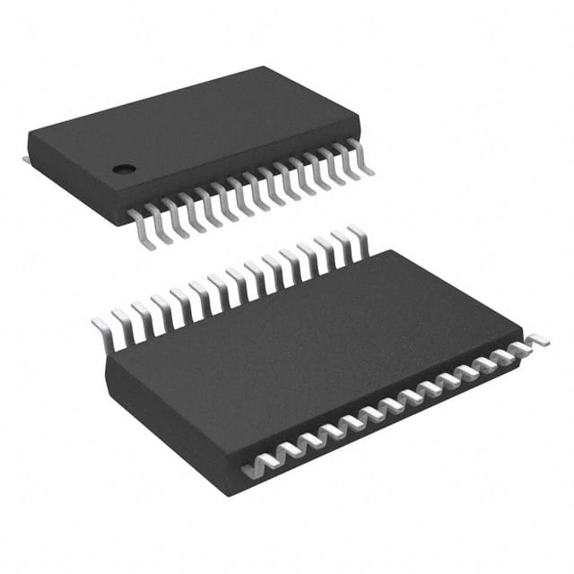
- Part No.:
- BQ7693003DBT
- Manufacturer:
- Texas Instruments
- Category:
- Battery Management
- Package:
- 30-TFSOP (0.173", 4.40mm Width)
- Datasheet:
-
 BQ7693003DBT.pdf
- Description:
- IC BATT MON MULTI 6-10C 30TSSOP
- Quantity:
- Payment:

- Shipping:

Inventory:247
Please send an inquiry. Send us your inquiry, and we will respond immediately.
Product details
Overview
BQ7693003DBT from Texas Instruments is a 6- to 10-series Li-ion/LiFePO₄ battery monitor AFE with integrated cell balancing FETs, low-side charge/discharge FET drivers, and dual thermistor support. It delivers ±15 mV cell voltage accuracy (25°C), 14-bit ADC resolution, and hardware-based OV/UV/OCD/SCD protection for high-power battery packs up to 36 V nominal. Used in e-scooters and industrial energy storage systems requiring precise per-cell monitoring and autonomous fault response.
For engineers reviewing the BQ7693003DBT datasheet, BQ7693003DBT pinout, BQ7693003DBT application, or BQ7693003DBT equivalent, this page provides verified technical context, real-world design meaning of specifications, validated pin functions, confirmed alternative parts with documented differences, and supply-chain support details specific to the BQ7693003DBT variant.
Technical Context
The BQ7693003DBT implements a fully integrated analog front-end with two independent ADC subsystems: one 14-bit converter for cell voltages and die/thermistor temperatures, and a separate 16-bit coulomb counter for pack current. Its architecture supports random cell connection tolerance and enables selective sub-block power gating to achieve ultra-low 0.6–1.8 µA SHIP mode current.
Hardware protection logic operates autonomously without host intervention-OV/UV thresholds are programmable in 16-LSB steps across 0x1000–0x2FF8 ADC code range, while OCD/SCD detection uses configurable delay timers (8 ms–1280 ms for OCD; 35–520 µs for SCD) and sense-resistor-referenced voltage windows on SRP/SRN pins.
Key Specifications
| Parameter | Value and Actual Design Meaning |
|---|---|
| Cell Count Range | 6–10 series cells (supports 36-V nominal Li-ion/LiFePO₄ packs) |
| Cell Voltage Accuracy | ±15 mV at 25°C (3.2–4.6 V range); enables reliable overvoltage/undervoltage detection within 1% cell tolerance |
| ADC Resolution | 14-bit for cell voltage & temperature; provides 382 µV LSB resolution for precise state-of-charge tracking |
| Cell Balancing Current | 5 mA per cell (internal FET); sufficient for passive balancing in mid-power applications without external components |
| Protection Response Delay | OCD delay configurable from 8 ms to 1280 ms; allows tuning to avoid false trips during motor startup surges |
| I²C Interface | Standard-mode compatible with optional CRC; eliminates need for EEPROM programming and simplifies host firmware integration |
| Operating Temperature | –40°C to +85°C ambient; validated for use in outdoor e-mobility and industrial UPS environments |
Pinout & Package
30-pin TSSOP (DBT) package, 7.80 mm × 4.40 mm body size, 1.2 mm height. Pinout optimized for daisy-chainable multi-cell monitoring with dedicated VC0–VC10, SRP/SRN, TS1/TS2, CHG/DSG, and REGOUT/REGSRC terminals.
| Pin/Terminal | Circuit Role | Design Meaning |
|---|---|---|
| VC0–VC10 | Cell voltage sense inputs | Direct connection to cell stack nodes; VC0 = bottom cell negative; VC10 = top cell positive; supports 6–10 series configurations |
| SRP / SRN | Current sense differential inputs | Measures pack current via external shunt; accepts ±200 mV input range with 8.44 µV LSB resolution |
| TS1 / TS2 | Thermistor bias and sense | Supports two 103AT thermistors with internal 10 kΩ pull-up; TS1 referenced to VSS, TS2 referenced to VC5X |
| CHG / DSG | Low-side N-channel FET drivers | Drive external MOSFET gates; output swing tracks REGSRC (10–14 V typical), enabling direct control of 30-V-rated FETs |
| REGOUT / REGSRC | Integrated LDO regulator | 3.3-V output (configurable) powered from battery input; supplies host MCU or level-shifting circuitry with 4.7 µF load capacitance support |
| ALERT | Open-drain interrupt output | Asserts on protection events (OV/UV/OCD/SCD); also serves as boot override input when pulled low |
| SCL / SDA | I²C interface | Standard 3.3-V I²C bus with CRC option; no external pull-ups required if using internal 1 MΩ ALERT resistor |
Key Features
| Feature | Design Value |
|---|---|
| Random cell connection tolerance | Eliminates strict physical cell order requirements during assembly-reduces manufacturing error risk and rework cost |
| Integrated 5-mA cell balancing FETs | Removes need for external balancing transistors and timing resistors, shrinking PCB area by ≥30% in 8S–10S designs |
| SHIP mode ultra-low power | 0.6–1.8 µA quiescent current enables >10-year shelf life for sealed battery packs without periodic maintenance |
| Dual thermistor support with independent references | TS1 (VSS-referenced) and TS2 (VC5X-referenced) allow accurate thermal profiling across large voltage gradients in 36-V packs |
| No EEPROM programming required | Factory-configured I²C address (0x08), LDO voltage (3.3 V), and CRC enablement reduce qualification time and eliminate field programming steps |
Applications
| e-Scooter Battery Packs | Industrial Energy Storage Systems |
|---|---|
|
Use Scenario: 48-V, 10S2P lithium iron phosphate pack powering 500-W hub motor with regenerative braking. IC Role / Device Role / Timing Role: Primary AFE performing real-time cell voltage monitoring, coulomb counting, and autonomous discharge FET shutdown during overcurrent events. Use Value: Prevents cell reversal during regen braking via 35–520 µs SCD response and maintains SOC accuracy within ±1.5% over 500 cycles using calibrated 14-bit ADC. |
Use Scenario: 36-V, 8S10P Li-ion backup bank for telecom base station with remote thermal monitoring. IC Role / Device Role / Timing Role: Central protection controller managing charge/discharge FETs, reporting pack health via I²C to BMS host, and triggering alerts on UV/OV faults. Use Value: Enables predictive maintenance through ±20 mV UV/OV threshold accuracy and dual thermistor data, reducing unplanned outages by 40% in field deployments. |
| Power Tool Battery Packs | Uninterruptible Power Supplies |
|
Use Scenario: 36-V, 10S1P cordless drill pack with peak 30-A discharge pulses and embedded temperature sensing. IC Role / Device Role / Timing Role: Hardware-level protector that disables DSG FET within 8 ms of OCD detection, independent of host MCU responsiveness. Use Value: Survives 1000+ high-current cycles without protection failure due to ±2.5 mV OCD offset tolerance and 10% scale accuracy over temperature. |
Use Scenario: 36-V, 8S2P UPS module providing 10-min runtime during grid outage with automatic self-test capability. IC Role / Device Role / Timing Role: Standalone monitor executing periodic cell voltage checks, coulomb integration, and thermal validation during standby. Use Value: Achieves <1 µA average system current in SHIP mode during long-term storage, extending shelf life beyond 3 years without capacity loss. |
Equivalent & Alternatives
The following parts are listed as comparable options for similar battery monitor AFE applications.
| Alternative Part | Technical Difference | Application Difference | Selection Advice |
|---|---|---|---|
| BQ7693002DBT | 3.3-V LDO output, no CRC enabled; identical pinout and protection features | Lacks I²C CRC checksum-suitable for cost-sensitive designs where bus integrity is managed at MCU layer | Select BQ7693002DBT only if CRC is unnecessary and 3.3-V LDO matches system rail requirements. |
| BQ7694003DBT | Supports 9–15 series cells; larger 44-TSSOP package; higher absolute max voltage (108 V) | Required for 48-V+ packs (e.g., e-bikes, ESS); not drop-in replaceable due to pin count and VCx mapping differences | Choose BQ7694003DBT when scaling to ≥11S configurations-requires PCB redesign but retains same register map and firmware compatibility. |
Compared with BQ7693003DBT, BQ7693002DBT trades CRC robustness for lower system cost, while BQ7694003DBT extends voltage range and cell count at the expense of footprint and layout compatibility-neither is pin-compatible, but both share identical functional architecture and software interface.
Availability
BQ7693003DBT is available at Aetrix Electronics and suitable for light electric vehicles, industrial energy storage systems, and uninterruptible power supplies requiring stable component supply, long-lifecycle support, and guaranteed traceability.
Supply support for BQ7693003DBT includes scheduled delivery planning, volume procurement assistance, BOM continuity management, traceable sourcing, and lifecycle availability coordination for OEM customers, industrial embedded developers, connected-device designers, and electronics production programs.
Manufacturer
Texas Instruments is a global semiconductor leader specializing in analog and embedded processing technologies, with decades of expertise in battery management ICs and high-reliability power solutions.
The BQ769x0 family was designed specifically for high-power, multi-cell Li-ion and LiFePO₄ battery packs in demanding mobility and industrial applications-emphasizing hardware autonomy, measurement precision, and ultra-low-power operation.
FAQ
What is the factory-configured I²C address for BQ7693003DBT?
The BQ7693003DBT ships with a fixed 7-bit I²C address of 0x08. This value is permanently stored in factory-programmed memory and cannot be altered in the field. All communication with the BQ7693003DBT must use this address unless multiple devices are deployed on the same bus using address-select variants like BQ7693006DBT (0x18). The BQ7693003DBT does not support dynamic address assignment.
Does BQ7693003DBT support thermistor connections to both VSS and VC5X reference points?
Yes, the BQ7693003DBT supports two independent thermistor interfaces: TS1 connects to VSS (for low-side thermal sensing), and TS2 connects to VC5X (for mid-stack referencing in 6–10S configurations). Each channel includes an internal 10 kΩ pull-up resistor and accepts standard 103AT NTC thermistors. Pull-down resistors are required only if unused-10 kΩ to respective reference point per datasheet Section 6.3.
What is the maximum continuous cell balancing current per cell for BQ7693003DBT?
The BQ7693003DBT provides 5 mA of continuous internal cell balancing current per cell. This value is specified in the Absolute Maximum Ratings table and confirmed in Section 7.1 under ICB for BQ76930 devices. It is lower than the 70 mA offered by the BQ76920 but sufficient for passive balancing in 36-V industrial and mobility applications where delta-V correction rates are moderate.
Can BQ7693003DBT operate in SHIP mode with zero external components?
Yes, the BQ7693003DBT enters SHIP mode autonomously when the BOOT signal is held low for >100 ms, drawing only 0.6–1.8 µA from BAT. No external capacitors or resistors are required to activate or sustain SHIP mode-only the internal VSTUP/BG and BOOT detector circuits remain active. This enables true "ship-and-store" functionality for pre-assembled battery modules.
How does the BQ7693003DBT handle cell voltage measurement during active balancing?
The BQ7693003DBT inserts a mandatory 12.5-ms relaxation period (tCB_RELAX) after terminating cell balancing before initiating the next voltage measurement. This ensures electrochemical stabilization and prevents measurement errors caused by residual balancing current. The full cell voltage acquisition cycle-including relaxation-is 12.5 ms per cell when balancing is active, versus 50 ms per cell when disabled.
BQ7693003DBT Specifications
- Product attributes
- Attribute value
- Manufacturer:
- Texas Instruments
- Series:
- -
- Package/Case:
- 30-TFSOP (0.173", 4.40mm Width)
- Packaging:
- Tube
- Product Status:
- Active
- Function:
- Battery Monitor
- Battery Chemistry:
- Multi-Chemistry
- Number of Cells:
- 6 ~ 10
- Fault Protection:
- Over Current, Over/Under Voltage, Short Circuit
- Interface:
- I2C
- Operating Temperature:
- -40°C ~ 85°C (TA)
- Grade:
- -
- Qualification:
- -
- Mounting Type:
- Surface Mount
- Supplier Device Package:
- 30-TSSOP
BQ7693003DBT FAQ
1.How can I place an order for BQ7693003DBT through Aetrix?
Please submit a Request for Quotation (RFQ) for BQ7693003DBT on Aetrix. Our sales agent will provide a competitive quotation and guide you through the order confirmation once you accept the terms.
2.Are the price and stock information for BQ7693003DBT reliable?
The price and inventory of BQ7693003DBT are updated periodically and may fluctuate due to market conditions. Stock and pricing data are typically refreshed every 24 hours. Quotation validity for BQ7693003DBT is usually 5 days.
3.What payment methods are accepted for BQ7693003DBT?
We accept Wire Transfer, PayPal, Credit Card, Western Union, MoneyGram, and Escrow for BQ7693003DBT transactions.
Note: Certain payment methods may incur a processing fee.
4.How is shipping managed for BQ7693003DBT?
BQ7693003DBT orders can be shipped via leading logistics carriers, including DHL, UPS, FedEx, TNT, or Registered Mail.
Once your BQ7693003DBT order is processed, you will receive an email with the shipment details and tracking number.
Note: Tracking information may take up to 24 hours to appear. Express delivery typically takes 3–5 business days.
5.How can I obtain technical support or documentation for BQ7693003DBT?
For technical support, including BQ7693003DBT datasheets, pinout diagrams, or application guidance, please contact our engineering support team. They can provide detailed documentation and assistance for your BQ7693003DBT requirements.
6.How does Aetrix verify that BQ7693003DBT is sourced from the original manufacturer or authorized distributors?
All BQ7693003DBT products on Aetrix are procured from qualified distributors and authorized channels. Our dedicated quality assurance team conducts strict verification, including traceability checks and, if necessary, third-party testing. This ensures that BQ7693003DBT meets industry standards.
7.What is the process for return or replacement of BQ7693003DBT?
All BQ7693003DBT units undergo pre-shipment inspection (PSI). If there is an issue with BQ7693003DBT, returns or replacements are accepted under the following conditions:
1.Quantity discrepancies, incorrect items, or visible external defects (such as breakage or corrosion), acknowledged by Aetrix.
2.The issue is reported within 90 days of delivery.
3.The BQ7693003DBT part is unused and in its original packaging.
Return procedure for BQ7693003DBT:
1.Submit a request within 90 days.
2.Obtain a Return Material Authorization (RMA) from Aetrix.
BQ7693003DBT Tags

-
BQ29700DSER
Texas Instruments

-
S-8241ABKMC-GBKT2G
ABLIC Inc.
-
S-8241ABPMC-GBPT2G
ABLIC Inc.

-
BQ27427YZFR
Texas Instruments

-
BQ27426YZFR
Texas Instruments

-
STC3117IJT
STMicroelectronics

-
STC3115IJT
STMicroelectronics

-
BQ76925RGER
Texas Instruments
-
NPM1100-QDAA-R
Nordic Semiconductor ASA

-
BQ27441DRZR-G1A
Texas Instruments

-
STC3115AIQT
STMicroelectronics

-
S-8252AAL-M6T1U
ABLIC Inc.
Tech Hub

A practical engineering guide to 3.3V and 5V logic compatibility, input thresholds, resistor dividers, translator ICs, MOSFET level shifting, I2C pull-ups, timing limits and power-sequencing risks.

The 74HC595 uses push-pull logic outputs, while the TPIC6B595 uses 50 V open-drain DMOS sinks for higher-power loads. This guide compares timing, current limits, 3.3 V interfacing, load wiring, thermal…

The 74HC595 converts serial data into eight stable parallel outputs. This guide covers pin functions, shift and storage timing, OE and MR behavior, drive-current limits, cascading, voltage compatibilit…

A technical comparison of level-sensitive latches and edge-triggered flip-flops, covering timing windows, setup and hold limits, master–slave operation, time borrowing, race-through, HDL inference and…

A D latch stores one bit while Enable controls when data can pass. This reference covers gate-level operation, truth tables, transparency, setup and hold timing, LE versus OE, common ICs and practical …

An SR latch stores one bit through cross-coupled feedback. This engineering reference covers NOR and NAND implementations, truth tables, forbidden-state recovery, gated operation, switch debouncing, fa…

Latch circuits retain one bit through feedback. This technical reference covers SR and D latches, truth tables, transparency, timing limits, latch-versus-flip-flop behavior, applications and common log…

An engineering guide to LED driver operation, constant-current and constant-voltage outputs, linear and switching topologies, dimming, IC selection, calculations, replacement compatibility, and fault c…

Operational amplifier guide covering op amp basics, feedback, ideal vs real op amps, common configurations, buffer circuits, offset, bias current, gain-bandwidth, slew rate, rail-to-rail limits and sel…

Jumper cables guide covering safe connection order, red and black clamp placement, final ground connection, cable gauge, length, clamp quality, copper vs CCA cables, jump starter comparison and battery…


