
 My Inquiry
 My Account


Texas Instruments BQ771825DPJR
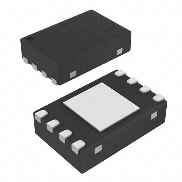
- Part No.:
- BQ771825DPJR
- Manufacturer:
- Texas Instruments
- Category:
- Battery Management
- Package:
- 8-WDFN Exposed Pad
- Datasheet:
-
 BQ771825DPJR.pdf
- Description:
- FAMILY 2-5S OVERVOLTAGE PROTECTO
- Quantity:
- Payment:

- Shipping:

Inventory:2,950
Please send an inquiry. Send us your inquiry, and we will respond immediately.
Product details
Overview
BQ771825DPJR from Texas Instruments is a dedicated overvoltage protection IC for 2- to 5-series Li-ion battery packs, featuring ±10 mV OVP accuracy, 3.950 V fixed overvoltage threshold, and N-channel open-drain active-low output with 3 s internal delay timer. It operates across –40°C to 110°C and consumes ≈1 µA quiescent current, enabling reliable cell-level monitoring in cordless power tools and e-bike battery management systems.
For engineers reviewing the BQ771825DPJR datasheet, BQ771825DPJR pinout, BQ771825DPJR application, or BQ771825DPJR equivalent, key selection criteria include its 3.950 V OVP threshold with 50 mV hysteresis, 3 s fault delay, NCH open-drain output drive capability, low 100 nA per-cell input leakage, and functional safety documentation support for ISO 26262-compliant designs.
Technical Context
The BQ771825DPJR independently monitors up to five differential cell voltages (V1–VSS through V5–V4) using precision internal references. Its overvoltage detection circuit compares each cell voltage against a fixed 3.950 V threshold with ±10 mV accuracy at 25°C and triggers an internal 3 s delay timer upon violation.
Upon timer expiration, the N-channel open-drain OUT pin pulls low to VSS (active-low), requiring an external pull-up resistor. The device supports Customer Test Mode (CTM) with sub-15 ms fault detection for production-line validation, and includes integrated RC filter interface support via RIN/CIN pins for noise-immune sensing.
Key Specifications
| Parameter | Value and Actual Design Meaning |
|---|---|
| OVP Threshold | 3.950 V ±10 mV at 25°C - sets precise cell overvoltage trip point for Li-ion chemistry |
| OVP Hysteresis | 50 mV - prevents chatter during recovery near threshold |
| Delay Timer | 3 s nominal - provides configurable fault response window before output activation |
| Supply Current | ≈1 µA when all cells below VOV - enables ultra-low-power standby in battery packs |
| Input Leakage | <100 nA per cell input - minimizes self-discharge impact on stacked cells |
| Operating Temp | –40°C to 110°C - supports industrial and automotive-grade battery pack environments |
| Output Type | NCH open-drain active-low - requires external pull-up; compatible with common BMS fault signaling buses |
Pinout & Package
Package: 8-pin WSON (DPJ), 3.00 mm × 4.00 mm, wettable flank, RoHS-compliant.
| Pin/Terminal | Circuit Role | Design Meaning |
|---|---|---|
| VDD | Power supply input | Unregulated 3–25 V supply; requires series resistor and bypass capacitor for noise filtering |
| V5 | Cell voltage sense input | Senses positive terminal of topmost (5th) cell in stack; connects to V5–V4 differential node |
| V4 | Cell voltage sense input | Senses positive terminal of 4th cell; connects to V4–V3 differential node |
| V3 | Cell voltage sense input | Senses positive terminal of 3rd cell; connects to V3–V2 differential node |
| V2 | Cell voltage sense input | Senses positive terminal of 2nd cell; connects to V2–V1 differential node |
| V1 | Cell voltage sense input | Senses positive terminal of lowest (1st) cell; connects to V1–VSS differential node |
| VSS | Ground reference | IC ground and negative terminal of bottom cell; must connect directly to PACK– |
| OUT | Fault signal output | N-channel open-drain active-low output; sinks current when OVP detected; requires external pull-up |
Key Features
| Feature | Design Value |
|---|---|
| Independent multi-cell monitoring | Simultaneous differential sensing of up to five cells without shared reference drift |
| Fixed-accuracy OVP | ±10 mV tolerance at 25°C ensures consistent trip points across production batches |
| Functional safety support | Documentation available for ISO 26262 ASIL-B system-level integration and FMEDA analysis |
| Customer Test Mode (CTM) | Reduces fault detection delay to <15 ms for rapid production-line verification of OVP timing |
| Low-leakage inputs | <100 nA per Vx pin preserves cell balance and extends shelf life in stored battery packs |
Applications
| Handheld Power Tools | Cordless Vacuum Cleaners |
|---|---|
Use Scenario: 18–20 V battery packs powering brushed/brushless motors with high transient current draw. IC Role / Device Role: Independent overvoltage monitor for each series cell to prevent Li-ion thermal runaway during fast charging or regenerative braking. Use Value: 3.950 V OVP threshold matches common 4S Li-ion configurations (15.8 V nominal), while 3 s delay allows safe charge termination without nuisance tripping. | Use Scenario: 20–25 V battery packs operating under variable load with frequent deep discharge cycles. IC Role / Device Role: Cell-level overvoltage protector interfaced with host MCU via open-drain fault line. Use Value: NCH open-drain output enables wired-OR fault bus architecture across multiple protection ICs; 1 µA quiescent current minimizes standby drain. |
| eBikes & eScooters | UPS Battery Backup |
Use Scenario: 36–48 V battery packs exposed to wide ambient temperature ranges (–20°C to 60°C). IC Role / Device Role: Primary overvoltage guard in redundant BMS architectures, working alongside cell balancing and temperature monitoring. Use Value: –40°C to 110°C operating range ensures reliability in outdoor vehicle enclosures; ±10 mV accuracy maintains tight voltage margins across temperature. | Use Scenario: 24–48 V sealed lead-acid or Li-ion backup systems requiring fail-safe shutdown on charger overvoltage. IC Role / Device Role: Standalone overvoltage cutoff device triggered by external charger output excursion. Use Value: Internal 3 s delay accommodates brief charger transients; 100 nA input leakage prevents measurable self-discharge during long-term standby. |
Equivalent & Alternatives
The following parts are listed as comparable options for similar overvoltage protection applications.
| Alternative Part | Technical Difference | Application Difference | Selection Advice |
|---|---|---|---|
| BQ771801DPJR | 4.275 V OVP threshold, 3 s delay, same NCH open-drain output | Targeted for higher-voltage 4S/5S Li-ion packs (17.1–21.4 V); less suitable for 3S packs with 3.95 V max cell voltage | Select BQ771801DPJR only if system requires 4.275 V trip point and maintains ≥0.325 V margin above typical 3.95 V full-charge cell voltage |
| BQ771823DPJR | 4.275 V OVP threshold, 3 s delay, NCH open-drain output, 300 mV hysteresis | Higher hysteresis reduces false trips in noisy environments but increases voltage recovery gap; same voltage range as BQ771801DPJR | Choose BQ771823DPJR where EMI immunity is critical and 300 mV hysteresis is acceptable for system recovery behavior |
Compared with BQ771825DPJR, BQ771801DPJR and BQ771823DPJR offer identical timing and output architecture but differ in OVP threshold (4.275 V vs. 3.950 V) and hysteresis (50 mV vs. 300 mV), making them unsuitable drop-in replacements without revalidation of cell voltage margins and recovery behavior.
Availability
BQ771825DPJR is available at Aetrix Electronics and suitable for handheld power tools, e-bikes, and UPS battery backup systems requiring stable component supply, long-lifecycle support, and functional safety documentation.
Supply support for BQ771825DPJR includes scheduled delivery planning, volume procurement assistance, BOM continuity management, traceable sourcing, and lifecycle availability coordination for OEM customers, industrial embedded developers, connected-device designers, and electronics production programs.
Manufacturer
Texas Instruments is a global semiconductor company delivering analog and embedded processing solutions, with leadership in battery management ICs and functional safety design resources.
The BQ7718 family is designed specifically for standalone overvoltage protection in multi-cell Li-ion battery packs, emphasizing precision, low power, and production-testability via Customer Test Mode.
FAQ
What is the overvoltage protection threshold of the BQ771825DPJR?
The BQ771825DPJR has a fixed overvoltage protection threshold of 3.950 V with ±10 mV accuracy at 25°C. This value is factory-trimmed and applies to each monitored cell voltage (V1–VSS through V5–V4). The device does not support user-programmable thresholds, and the 3.950 V setting is optimized for 3S Li-ion configurations where individual cell voltage must not exceed 3.95 V during charging or operation. BQ771825DPJR maintains this specification across its full operating temperature range.
Does the BQ771825DPJR support 2-cell, 3-cell, 4-cell, and 5-cell battery configurations?
Yes, the BQ771825DPJR supports 2- to 5-series Li-ion battery configurations. It monitors up to five differential cell voltages (V1–VSS, V2–V1, V3–V2, V4–V3, V5–V4) and remains fully functional with fewer cells by leaving unused Vx pins unconnected or tied appropriately. For example, in a 3S configuration, only V1, V2, V3, and VSS are used; V4 and V5 are left floating. The internal sensing circuitry automatically adapts without configuration changes. BQ771825DPJR's architecture eliminates the need for external multiplexing or reconfiguration between pack sizes.
What type of output driver does the BQ771825DPJR use, and how should it be interfaced?
The BQ771825DPJR uses an N-channel open-drain active-low output (OUT pin). When an overvoltage condition is detected and the 3 s delay expires, the OUT pin pulls low to VSS; otherwise, it presents high-impedance. An external pull-up resistor to PACK+ or another logic-rail voltage is mandatory. Typical values range from 10 kΩ to 100 kΩ depending on bus capacitance and noise immunity requirements. This output type enables wired-OR fault signaling across multiple protection devices and ensures compatibility with standard BMS microcontroller interrupt inputs. BQ771825DPJR does not provide active-high drive capability.
How does the Customer Test Mode (CTM) function in the BQ771825DPJR?
Customer Test Mode (CTM) in the BQ771825DPJR reduces the overvoltage fault detection delay from 3 s to less than 15 ms for production-line testing. CTM is activated by applying VDD at least 10 V higher than the V5 pin voltage - for example, if V5 = 12 V, then VDD ≥ 22 V. The mode exits automatically when the VDD-to-V5 differential falls below 10 V. CTM preserves all other functional behaviors, including OVP threshold and hysteresis, allowing full validation of timing performance without modifying hardware. BQ771825DPJR documentation confirms CTM is supported across all variants in the BQ7718xy family.
Is the BQ771825DPJR qualified for functional safety applications?
Yes, the BQ771825DPJR is functional safety-capable, with documentation available to aid ISO 26262 system-level design. Texas Instruments provides failure modes, effects, and diagnostic analysis (FMEDA) data, safety manuals, and diagnostic coverage reports for the BQ7718 family. While BQ771825DPJR itself is not ASIL-certified, its architecture - including independent cell monitoring, accurate OVP, and predictable timing - supports ASIL-B decomposition in battery management systems. Functional safety qualification requires system-level integration and validation; BQ771825DPJR serves as a foundational safety element within that architecture.
BQ771825DPJR Specifications
- Product attributes
- Attribute value
- Manufacturer:
- Texas Instruments
- Series:
- -
- Package/Case:
- 8-WDFN Exposed Pad
- Packaging:
- Tape & Reel (TR)
- Product Status:
- Active
- Function:
- Battery Protection
- Battery Chemistry:
- Lithium Ion
- Number of Cells:
- 2 ~ 5
- Fault Protection:
- Over Voltage
- Interface:
- -
- Operating Temperature:
- -40°C ~ 85°C
- Grade:
- -
- Qualification:
- -
- Mounting Type:
- Surface Mount
- Supplier Device Package:
- 8-WSON (3x4)
BQ771825DPJR FAQ
1.How can I place an order for BQ771825DPJR through Aetrix?
Please submit a Request for Quotation (RFQ) for BQ771825DPJR on Aetrix. Our sales agent will provide a competitive quotation and guide you through the order confirmation once you accept the terms.
2.Are the price and stock information for BQ771825DPJR reliable?
The price and inventory of BQ771825DPJR are updated periodically and may fluctuate due to market conditions. Stock and pricing data are typically refreshed every 24 hours. Quotation validity for BQ771825DPJR is usually 5 days.
3.What payment methods are accepted for BQ771825DPJR?
We accept Wire Transfer, PayPal, Credit Card, Western Union, MoneyGram, and Escrow for BQ771825DPJR transactions.
Note: Certain payment methods may incur a processing fee.
4.How is shipping managed for BQ771825DPJR?
BQ771825DPJR orders can be shipped via leading logistics carriers, including DHL, UPS, FedEx, TNT, or Registered Mail.
Once your BQ771825DPJR order is processed, you will receive an email with the shipment details and tracking number.
Note: Tracking information may take up to 24 hours to appear. Express delivery typically takes 3–5 business days.
5.How can I obtain technical support or documentation for BQ771825DPJR?
For technical support, including BQ771825DPJR datasheets, pinout diagrams, or application guidance, please contact our engineering support team. They can provide detailed documentation and assistance for your BQ771825DPJR requirements.
6.How does Aetrix verify that BQ771825DPJR is sourced from the original manufacturer or authorized distributors?
All BQ771825DPJR products on Aetrix are procured from qualified distributors and authorized channels. Our dedicated quality assurance team conducts strict verification, including traceability checks and, if necessary, third-party testing. This ensures that BQ771825DPJR meets industry standards.
7.What is the process for return or replacement of BQ771825DPJR?
All BQ771825DPJR units undergo pre-shipment inspection (PSI). If there is an issue with BQ771825DPJR, returns or replacements are accepted under the following conditions:
1.Quantity discrepancies, incorrect items, or visible external defects (such as breakage or corrosion), acknowledged by Aetrix.
2.The issue is reported within 90 days of delivery.
3.The BQ771825DPJR part is unused and in its original packaging.
Return procedure for BQ771825DPJR:
1.Submit a request within 90 days.
2.Obtain a Return Material Authorization (RMA) from Aetrix.
BQ771825DPJR Tags

-
BQ29700DSER
Texas Instruments

-
S-8241ABKMC-GBKT2G
ABLIC Inc.
-
S-8241ABPMC-GBPT2G
ABLIC Inc.

-
BQ27427YZFR
Texas Instruments

-
BQ27426YZFR
Texas Instruments

-
STC3117IJT
STMicroelectronics

-
STC3115IJT
STMicroelectronics

-
BQ76925RGER
Texas Instruments
-
NPM1100-QDAA-R
Nordic Semiconductor ASA

-
BQ27441DRZR-G1A
Texas Instruments

-
STC3115AIQT
STMicroelectronics

-
S-8252AAL-M6T1U
ABLIC Inc.
Tech Hub

A practical engineering guide to 3.3V and 5V logic compatibility, input thresholds, resistor dividers, translator ICs, MOSFET level shifting, I2C pull-ups, timing limits and power-sequencing risks.

The 74HC595 uses push-pull logic outputs, while the TPIC6B595 uses 50 V open-drain DMOS sinks for higher-power loads. This guide compares timing, current limits, 3.3 V interfacing, load wiring, thermal…

The 74HC595 converts serial data into eight stable parallel outputs. This guide covers pin functions, shift and storage timing, OE and MR behavior, drive-current limits, cascading, voltage compatibilit…

A technical comparison of level-sensitive latches and edge-triggered flip-flops, covering timing windows, setup and hold limits, master–slave operation, time borrowing, race-through, HDL inference and…

A D latch stores one bit while Enable controls when data can pass. This reference covers gate-level operation, truth tables, transparency, setup and hold timing, LE versus OE, common ICs and practical …

An SR latch stores one bit through cross-coupled feedback. This engineering reference covers NOR and NAND implementations, truth tables, forbidden-state recovery, gated operation, switch debouncing, fa…

Latch circuits retain one bit through feedback. This technical reference covers SR and D latches, truth tables, transparency, timing limits, latch-versus-flip-flop behavior, applications and common log…

An engineering guide to LED driver operation, constant-current and constant-voltage outputs, linear and switching topologies, dimming, IC selection, calculations, replacement compatibility, and fault c…

Operational amplifier guide covering op amp basics, feedback, ideal vs real op amps, common configurations, buffer circuits, offset, bias current, gain-bandwidth, slew rate, rail-to-rail limits and sel…

Jumper cables guide covering safe connection order, red and black clamp placement, final ground connection, cable gauge, length, clamp quality, copper vs CCA cables, jump starter comparison and battery…


