
 My Inquiry
 My Account


Texas Instruments BQ77910ADBTR
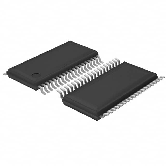
- Part No.:
- BQ77910ADBTR
- Manufacturer:
- Texas Instruments
- Category:
- Battery Management
- Package:
- 38-TFSOP (0.173", 4.40mm Width)
- Datasheet:
-
 BQ77910ADBTR.pdf
- Description:
- IC BATT LI-ION 4-10C 38TSSOP
- Quantity:
- Payment:

- Shipping:

Inventory:3,530
Please send an inquiry. Send us your inquiry, and we will respond immediately.
Product details
Overview
BQ77910ADBTR from Texas Instruments is a multi-cell lithium-ion/polymer battery protection and cell balancing IC designed for 4- to 10-series battery packs. It provides individual cell-voltage monitoring (VC1–VC11), internal 50-mA automatic cell balancing, low-side NMOS FET gate drive for charge/discharge control, and integrated 3.3-V micro-power LDO regulator. It is used in cordless power tools, electric bikes, and UPS systems requiring precise, programmable safety protection.
For engineers reviewing the BQ77910ADBTR datasheet, BQ77910ADBTR pinout, BQ77910ADBTR application, or BQ77910ADBTR equivalent, key selection considerations include its TSSOP-38 package, 50 µA typical normal-mode supply current, 5.6 V to 43.75 V operating supply range, programmable overvoltage/undervoltage thresholds, and EEPROM-configurable delay times for safety events.
Technical Context
The BQ77910ADBTR implements a fully programmable protection architecture with non-volatile EEPROM storage for threshold and timing settings across five safety functions: cell overvoltage, undervoltage, discharge overcurrent, discharge short circuit, and charge short circuit. Its analog front-end supports variable-gain (×1 or ×5) current sensing compatible with 1-mΩ to 5-mΩ sense resistors.
It integrates dual low-side NMOS gate drivers (CHG and DSG pins) with regulated 11–14 V gate drive under full regulation and dropout-mode operation down to 6.4 V BAT. The device uses substrate-referenced analog grounds (VSS1/VSS2), separate thermistor bias (VTSB), and open-cell detection logic that samples each cell with 7.5-minute balancing intervals and 4×N-second fault-check cycles.
Key Specifications
| Parameter | Value and Actual Design Meaning |
|---|---|
| Cell Count Support | 4- to 10-series Li-ion/Li-polymer cells - enables direct integration into mid-to-high voltage battery packs without external multiplexing. |
| Supply Voltage Range | 5.6 V to 43.75 V - covers nominal 4S (14.8 V) through 10S (37 V) configurations with headroom for charging transients. |
| Normal Mode Supply Current | 50 µA typical - minimizes quiescent drain on battery during standby, extending pack shelf life. |
| Cell Balancing Current | 50 mA internal - allows passive balancing without external FETs; requires external series resistance to limit IC power dissipation. |
| LDO Output | 3.3 V ±0.25 V at 10 mA - powers external thermistors or logic; includes thermal shutdown and short-circuit current limiting (20–45 mA). |
| Protection Threshold Accuracy | ±50 mV OV/UV at 0°C–50°C - ensures reliable cell voltage monitoring within tight safety margins for high-reliability applications. |
| Gate Drive Rise/Fall Time | 90–140 µs (CL = 50 nF) - supports fast FET switching while maintaining EMI control and robustness against parasitic ringing. |
Pinout & Package
Package: 38-pin TSSOP (9.70 mm × 4.40 mm), lead pitch 0.5 mm, exposed pad not specified for thermal connection.
| Pin/Terminal | Circuit Role | Design Meaning |
|---|---|---|
| BAT | High-side power supply input | Connected to most-positive cell terminal; supplies internal regulators and gate drivers; rated up to 43.75 V. |
| VC1–VC10 | Cell voltage sense inputs | Differential inputs for monitoring 1st through 10th most-positive cells; VC11 is dedicated to most-negative cell (BAT–). |
| VC11 | Most-negative cell reference | Serves as analog ground reference for cell stack; must connect directly to pack's lowest potential point. |
| SENSE(+), SENSE(–) | Current-sense differential inputs | Accept bidirectional current measurement across external shunt; support ×1/×5 gain selection for 1–5 mΩ resistors. |
| CHG, DSG | Low-side NMOS gate drivers | Drive external N-channel FETs for charge and discharge path control; output swing regulated to ~11–14 V (BAT ≥ 10 V). |
| VREG | 3.3-V LDO output | Powers external thermistors or logic; requires 1-µF ceramic capacitor; shuts down in shutdown mode to reduce leakage. |
| TS, VTSB | Thermistor interface | VTSB supplies bias current to NTC; TS reads ratiometric voltage; supports open/short/fault detection with 4-s sampling interval. |
| SCLK, SDATA | EEPROM programming interface | 2-wire serial interface (≤50 kHz); open-drain SDATA; used only for factory or development configuration - not runtime communication. |
| ZEDE | Zero-delay test mode enable | When pulled high, disables protection delays and enables serial interface; must be tied to VSS in production for normal operation. |
| NC (Pins 2,4,30,35,37) | No-connect terminals | Must remain unconnected; routing or soldering to NC pins may cause functional failure or undefined behavior. |
Key Features
| Feature | Design Value |
|---|---|
| Programmable protection thresholds | OV/UV thresholds adjustable from 2.8 V–4.375 V / 1.4 V–2.9 V in 25/100 mV steps; enables customization per cell chemistry and aging profile. |
| Configurable balancing schedule | Cell balancing can be enabled continuously, only during charge, or disabled - optimizing energy use and thermal management. |
| Split power-path MOSFET control | Independent CHG and DSG outputs allow separate charge/discharge FETs - essential for bidirectional energy flow in regenerative systems. |
| Open-cell and thermistor fault detection | Automated 4×N-second open-cell check and ratiometric TS monitoring detect broken sense lines or failed NTCs before pack deployment. |
| EEPROM-based configuration persistence | All protection settings stored in non-volatile memory; retains values across power cycles and brownouts without external backup. |
Applications
| Cordless Power Tools | Electric Bikes |
|---|---|
|
Use Scenario: High-current, intermittent load cycling during drilling, cutting, or hammering with rapid temperature rise and voltage sag. IC Role / Device Role / Timing Role: Monitors per-cell voltage during 30-A+ discharge pulses; triggers DSG FET cutoff within <2.25 s if any cell drops below 2.5 V. Use Value: Prevents deep discharge of weakest cell during burst loads, preserving cycle life and avoiding irreversible capacity loss. |
Use Scenario: Regenerative braking and hill-climbing demand asymmetric charge/discharge currents and thermal stress across 13–48 V battery packs. IC Role / Device Role / Timing Role: Uses independent CHG/DSG drivers to manage bidirectional FETs; balances cells at 50 mA during charging to maintain ≤50 mV inter-cell variance. Use Value: Enables safe regen without overcharging top cells, extending usable pack capacity by >8% over unbalanced operation. |
| UPS Systems | Light Electric Vehicles (LEV) |
|
Use Scenario: Extended standby with infrequent deep discharge events, requiring ultra-low quiescent current and long-term reliability. IC Role / Device Role / Timing Role: Operates in 50 µA normal mode; enters 3 µA shutdown when pack voltage falls below UV threshold and CPCKN floats. Use Value: Reduces annual self-discharge contribution to <0.3% - critical for 5-year field deployments without maintenance. |
Use Scenario: Compact, air-cooled battery packs in scooters and e-bikes where space constraints limit external balancing components. IC Role / Device Role / Timing Role: Integrates 50-mA balancing, 3.3-V LDO, and 1-mΩ-compatible sensing in single TSSOP-38 package - eliminates 3–4 discrete ICs. Use Value: Cuts BOM count by 35% and PCB area by 40% versus discrete protection + balancing solutions. |
Equivalent & Alternatives
The following parts are listed as comparable options for similar battery protection applications.
| Alternative Part | Technical Difference | Application Difference | Selection Advice |
|---|---|---|---|
| BQ77915ADBTR | Supports 5–15-series cells; adds integrated high-side charge FET driver; higher max BAT voltage (60 V); same TSSOP-38 package. | Required for >10S packs or designs needing active charge path control without external high-side driver. | Select BQ77915ADBTR when scaling beyond 10S or requiring integrated high-side charge control - not drop-in compatible due to pin function changes. |
| BD750L5GUL-E2 | 4–5S standalone protector (no balancing); 2.5- to 26-V range; 3.3-V LDO; 12-pin WLCSP; no EEPROM programmability. | Suitable for cost-sensitive, low-cell-count applications where fixed thresholds and no balancing suffice. | Choose BD750L5GUL-E2 for simple 4S/5S tools or medical devices where programmability and balancing are unnecessary. |
Compared with BQ77910ADBTR, the BQ77915ADBTR extends cell count and adds high-side drive but requires layout revision, while the BD750L5GUL-E2 reduces size and cost at the expense of configurability and balancing - making BQ77910ADBTR optimal for 4–10S balanced, field-programmable industrial packs.
Availability
BQ77910ADBTR is available at Aetrix Electronics and suitable for cordless power tools, electric bikes, and UPS systems requiring stable component supply throughout extended production lifecycles.
Supply support for BQ77910ADBTR includes scheduled delivery planning, volume procurement assistance, BOM continuity management, traceable sourcing, and lifecycle availability coordination for OEM customers, industrial embedded developers, connected-device designers, and electronics production programs.
Manufacturer
Texas Instruments is a global semiconductor leader specializing in analog, embedded processing, and power management technologies with decades of battery management system expertise.
The bq779xx family was engineered specifically for high-reliability, multi-cell Li-ion/Li-polymer pack protection - emphasizing programmable safety, integrated balancing, and robust fault diagnostics for industrial and mobility applications.
FAQ
Is BQ77910ADBTR recommended for new designs?
No, BQ77910ADBTR is marked "Not Recommended for New Designs" by Texas Instruments as of the October 2014 datasheet revision. It remains available for legacy support and existing production, but TI recommends evaluating newer alternatives like BQ77915ADBTR or BQ769x2 series for new projects requiring enhanced features, longer lifecycle, or updated safety certifications.
What is the maximum number of cells supported by BQ77910ADBTR?
The BQ77910ADBTR supports 4- to 10-series lithium-ion or lithium-polymer cells, as confirmed by its 11 dedicated cell-sense inputs (VC1–VC10 plus VC11 for BAT–). This configuration enables direct monitoring of up to 10 stacked cells without external multiplexers or voltage dividers.
Does BQ77910ADBTR include internal cell balancing capability?
Yes, BQ77910ADBTR integrates internal 50-mA cell balancing circuits per monitored cell. Balancing is programmable via EEPROM to operate continuously, only during charge, or disabled - and requires external series resistance to ensure the IC's internal power dissipation stays within safe limits.
Can BQ77910ADBTR drive both charge and discharge FETs independently?
Yes, BQ77910ADBTR provides two independent low-side NMOS gate drivers: CHG pin controls the charge FET, and DSG pin controls the discharge FET. This split power-path architecture enables true bidirectional protection - critical for applications with regenerative braking or external charger control.
What is the purpose of the ZEDE pin on BQ77910ADBTR?
The ZEDE (Zero Delay Enable) pin on BQ77910ADBTR activates test mode: when pulled high, it disables all protection delay timers and enables the serial programming interface. In production, ZEDE must be hard-connected to VSS to ensure standard delay behavior and prevent unintended configuration access.
BQ77910ADBTR Specifications
- Product attributes
- Attribute value
- Manufacturer:
- Texas Instruments
- Series:
- -
- Package/Case:
- 38-TFSOP (0.173", 4.40mm Width)
- Packaging:
- Tape & Reel (TR)
- Product Status:
- Not For New Designs
- Function:
- Multi-Function Controller
- Battery Chemistry:
- Lithium Ion/Polymer
- Number of Cells:
- 4 ~ 10
- Fault Protection:
- Over Current, Over Temperature, Over/Under Voltage, Short Circuit
- Interface:
- I2C
- Operating Temperature:
- -25°C ~ 85°C (TA)
- Grade:
- -
- Qualification:
- -
- Mounting Type:
- Surface Mount
- Supplier Device Package:
- 38-TSSOP
BQ77910ADBTR FAQ
1.How can I place an order for BQ77910ADBTR through Aetrix?
Please submit a Request for Quotation (RFQ) for BQ77910ADBTR on Aetrix. Our sales agent will provide a competitive quotation and guide you through the order confirmation once you accept the terms.
2.Are the price and stock information for BQ77910ADBTR reliable?
The price and inventory of BQ77910ADBTR are updated periodically and may fluctuate due to market conditions. Stock and pricing data are typically refreshed every 24 hours. Quotation validity for BQ77910ADBTR is usually 5 days.
3.What payment methods are accepted for BQ77910ADBTR?
We accept Wire Transfer, PayPal, Credit Card, Western Union, MoneyGram, and Escrow for BQ77910ADBTR transactions.
Note: Certain payment methods may incur a processing fee.
4.How is shipping managed for BQ77910ADBTR?
BQ77910ADBTR orders can be shipped via leading logistics carriers, including DHL, UPS, FedEx, TNT, or Registered Mail.
Once your BQ77910ADBTR order is processed, you will receive an email with the shipment details and tracking number.
Note: Tracking information may take up to 24 hours to appear. Express delivery typically takes 3–5 business days.
5.How can I obtain technical support or documentation for BQ77910ADBTR?
For technical support, including BQ77910ADBTR datasheets, pinout diagrams, or application guidance, please contact our engineering support team. They can provide detailed documentation and assistance for your BQ77910ADBTR requirements.
6.How does Aetrix verify that BQ77910ADBTR is sourced from the original manufacturer or authorized distributors?
All BQ77910ADBTR products on Aetrix are procured from qualified distributors and authorized channels. Our dedicated quality assurance team conducts strict verification, including traceability checks and, if necessary, third-party testing. This ensures that BQ77910ADBTR meets industry standards.
7.What is the process for return or replacement of BQ77910ADBTR?
All BQ77910ADBTR units undergo pre-shipment inspection (PSI). If there is an issue with BQ77910ADBTR, returns or replacements are accepted under the following conditions:
1.Quantity discrepancies, incorrect items, or visible external defects (such as breakage or corrosion), acknowledged by Aetrix.
2.The issue is reported within 90 days of delivery.
3.The BQ77910ADBTR part is unused and in its original packaging.
Return procedure for BQ77910ADBTR:
1.Submit a request within 90 days.
2.Obtain a Return Material Authorization (RMA) from Aetrix.
BQ77910ADBTR Tags

-
BQ29700DSER
Texas Instruments

-
S-8241ABKMC-GBKT2G
ABLIC Inc.
-
S-8241ABPMC-GBPT2G
ABLIC Inc.

-
BQ27427YZFR
Texas Instruments

-
BQ27426YZFR
Texas Instruments

-
STC3117IJT
STMicroelectronics

-
STC3115IJT
STMicroelectronics

-
BQ76925RGER
Texas Instruments
-
NPM1100-QDAA-R
Nordic Semiconductor ASA

-
BQ27441DRZR-G1A
Texas Instruments

-
STC3115AIQT
STMicroelectronics

-
S-8252AAL-M6T1U
ABLIC Inc.
Tech Hub

A practical engineering guide to 3.3V and 5V logic compatibility, input thresholds, resistor dividers, translator ICs, MOSFET level shifting, I2C pull-ups, timing limits and power-sequencing risks.

The 74HC595 uses push-pull logic outputs, while the TPIC6B595 uses 50 V open-drain DMOS sinks for higher-power loads. This guide compares timing, current limits, 3.3 V interfacing, load wiring, thermal…

The 74HC595 converts serial data into eight stable parallel outputs. This guide covers pin functions, shift and storage timing, OE and MR behavior, drive-current limits, cascading, voltage compatibilit…

A technical comparison of level-sensitive latches and edge-triggered flip-flops, covering timing windows, setup and hold limits, master–slave operation, time borrowing, race-through, HDL inference and…

A D latch stores one bit while Enable controls when data can pass. This reference covers gate-level operation, truth tables, transparency, setup and hold timing, LE versus OE, common ICs and practical …

An SR latch stores one bit through cross-coupled feedback. This engineering reference covers NOR and NAND implementations, truth tables, forbidden-state recovery, gated operation, switch debouncing, fa…

Latch circuits retain one bit through feedback. This technical reference covers SR and D latches, truth tables, transparency, timing limits, latch-versus-flip-flop behavior, applications and common log…

An engineering guide to LED driver operation, constant-current and constant-voltage outputs, linear and switching topologies, dimming, IC selection, calculations, replacement compatibility, and fault c…

Operational amplifier guide covering op amp basics, feedback, ideal vs real op amps, common configurations, buffer circuits, offset, bias current, gain-bandwidth, slew rate, rail-to-rail limits and sel…

Jumper cables guide covering safe connection order, red and black clamp placement, final ground connection, cable gauge, length, clamp quality, copper vs CCA cables, jump starter comparison and battery…


