
 My Inquiry
 My Account


Texas Instruments BUF08630RGWT
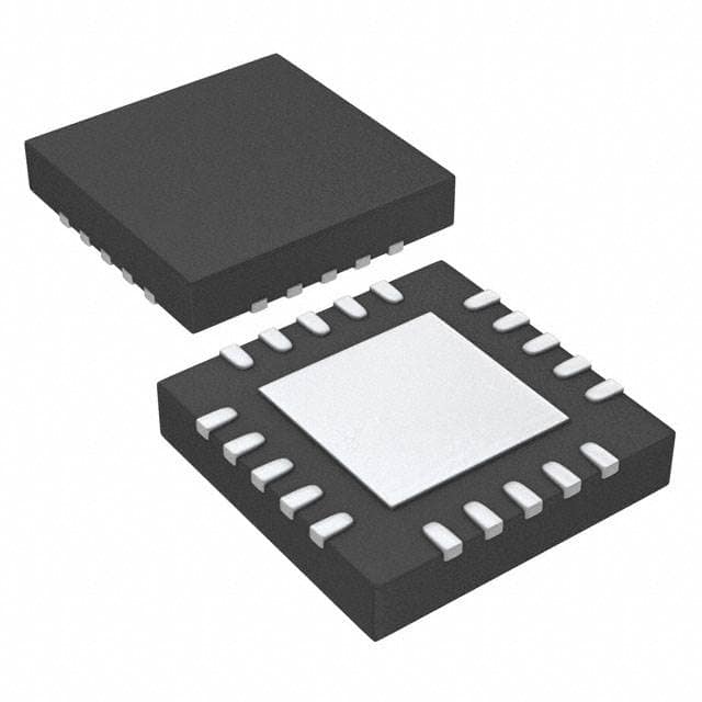
- Part No.:
- BUF08630RGWT
- Manufacturer:
- Texas Instruments
- Category:
- Video Amps and Modules
- Package:
- 20-VQFN Exposed Pad
- Datasheet:
-
 BUF08630RGWT.pdf
- Description:
- IC AMP TFT-LCD 20VQFN
- Quantity:
- Payment:

- Shipping:

Inventory:247
Please send an inquiry. Send us your inquiry, and we will respond immediately.
Product details
Overview
BUF08630 from Texas Instruments is an 8-channel programmable gamma-voltage generator and high-slew-rate VCOM driver with integrated two-bank nonvolatile memory, 10-bit DAC resolution, rail-to-rail output (±150 mV at 10 mA), and 45 V/μs VCOM slew rate-designed for TFT-LCD reference voltage generation in display timing controllers.
For engineers reviewing the BUF08630 datasheet, BUF08630 pinout, BUF08630 application, or BUF08630 equivalent, this page delivers verified electrical specs, bank-selectable memory architecture, VSH/VS supply sequencing requirements, and real-world gamma curve switching use cases-not generic analog buffer descriptions.
Technical Context
The BUF08630 implements dual independent 16× rewritable OTP memory banks (BANK0/BANK1) selected via BKSEL pin, enabling dynamic gamma curve switching without reprogramming. Each bank stores full 10-bit codes for eight gamma outputs (OUT1–OUT8) and one VCOM channel.
It uses a double-buffered DAC register structure supporting two update modes: immediate per-channel update (bit-15 = 1) or simultaneous multi-channel update (final write sets bit-15 = 1). The VCOM amplifier operates with 1/2 AVDD topology (VSH) and supports up to 400 mA continuous sink/source under defined load conditions.
Key Specifications
| Parameter | Value and Actual Design Meaning |
|---|---|
| Resolution | 10-bit DAC for all 8 gamma channels and VCOM output-enables 1024-step fine-tuning of LCD grayscale voltage levels. |
| VCOM Slew Rate | 45 V/μs-supports fast VCOM settling during frame-rate transitions in high-refresh-rate displays. |
| Rail-to-Rail Output | Swings to within 150 mV of supply rails at 10 mA load-ensures full dynamic range utilization across VS (9–20 V) and VSH (½ VS) rails. |
| Memory Banks | Two independent 16× rewritable OTP banks-allows storage and instant switching between two distinct gamma curves (e.g., sRGB and Adobe RGB). |
| Two-Wire Interface | Supports 400 kHz (Fast Mode) and 3.4 MHz (High-Speed Mode)-enables rapid factory calibration or runtime gamma adjustment. |
| Supply Range | Analog supply: 9 V to 20 V (VS); Digital supply: 2 V to 5.5 V (VSD); VSH must be ≤½ VS-dictates strict power-up sequencing (VSD → VCOM-VS/VS → VSH). |
| Output Current | VCOM: ±400 mA max; Gamma outputs: ±300 mA max-meets peak current demands of large-panel LCD bias networks. |
Pinout & Package
BUF08630 is housed in a 20-pin VQFN package (RGW) with exposed thermal pad soldered to GND. Package dimensions: 3.5 mm × 3.5 mm × 0.8 mm, 0.5 mm pitch.
| Pin/Terminal | Circuit Role | Design Meaning |
|---|---|---|
| OUT1–OUT8 | Gamma DAC outputs | Eight buffered analog outputs; OUT1–OUT4 swing high toward VS, OUT5–OUT8 swing low toward GND/VSH-enables split-rail gamma distribution. |
| VCOM-OUT | VCOM driver output | High-current, high-slew-rate output driving common electrode of LCD panel; requires external feedback via VCOM-FB. |
| VCOM-FB | VCOM amplifier feedback | Connects to VCOM-OUT through resistive divider-sets closed-loop gain and output voltage accuracy. |
| VCOM-VS | VCOM amplifier supply | Must be powered simultaneously with or before VS; mismatch causes analog switch damage. |
| VS | Main analog supply | 9–20 V input powering gamma buffers and VCOM amplifier core; powers OUT1–OUT4 high-side section. |
| VSH | Half-supply reference | Connected to ½ VS; defines mid-rail for OUT5–OUT8 and VCOM amplifier common-mode range. |
| SDA / SCL | Two-wire interface I/O | Open-drain, 3.4 MHz capable; A0 pin selects slave address (74h or 75h) for multi-device bus configuration. |
| BKSEL | Memory bank selector | Logic-high selects BANK1; logic-low selects BANK0; state change triggers immediate load of corresponding bank's values to DAC registers. |
| GND / DGND | Analog & digital ground | Separate AGND (pin 4) and DGND (pin 16 NC not used) recommended; exposed thermal pad tied to AGND for thermal management. |
| VSD | Digital supply | 2–5.5 V logic supply; must power up first to prevent latch-up or excessive quiescent current during analog supply ramp. |
Key Features
| Feature | Design Value |
|---|---|
| Two independent OTP memory banks | Enables zero-latency gamma curve switching in production test or field firmware updates-no reprogramming delay. |
| 1/2 AVDD topology with VSH pin | Allows OUT5–OUT8 to operate referenced to mid-supply, reducing headroom requirements and improving noise immunity in split-rail LCD bias designs. |
| Double-buffered DAC registers | Supports atomic multi-channel updates-prevents visual artifacts during gamma/VCOM synchronization in active matrix displays. |
| 45 V/μs VCOM slew rate | Meets <5 μs settling time requirement for 60+ Hz refresh rates in 4K/UHD panels with large capacitive loads. |
| Programmable VCOM limits (0–960 code) | Restricts VCOM output range to match amplifier input common-mode window-prevents clipping while preserving 10-bit resolution. |
| 16× OTP write endurance | Supports panel-specific calibration during manufacturing and post-deployment rework-exceeds typical LCD module lifetime requirements. |
Applications
| Mobile Display Calibration | TFT-LCD TV Bias Generation |
|---|---|
|
Use Scenario: Factory calibration of smartphone/tablet LCD panels using automated optical testers. IC Role / Device Role / Timing Role: Generates precise gamma reference voltages (OUT1–OUT8) and dynamic VCOM level synchronized to timing controller frame pulses. Use Value: Eliminates need for external DACs and op-amps; 10-bit resolution and 16× OTP writes enable per-panel tuning and yield recovery. |
Use Scenario: Generating 8 gamma references and VCOM for 55-inch 4K LCD TV with local dimming backlight. IC Role / Device Role / Timing Role: High-current VCOM driver (400 mA) and rail-to-rail gamma buffers replace discrete solutions, reducing BOM count by 12+ components. Use Value: 45 V/μs slew rate ensures VCOM stability during rapid brightness transitions; dual memory banks support picture mode switching (Cinema/Standard/Sports). |
| Automotive Instrument Cluster | Industrial HMI Display |
|
Use Scenario: Wide-temperature (-40°C to +95°C) LCD biasing in automotive digital dashboards with sunlight readability requirements. IC Role / Device Role / Timing Role: Delivers stable gamma and VCOM under varying battery voltage (9–16 V) and ambient temperature; VSH pin enables robust mid-rail referencing. Use Value: ±25 μV/°C VCOM output drift ensures consistent contrast ratio across operating range; OTP memory retains calibration after ignition cycle. |
Use Scenario: Medical or industrial control panel requiring ESD-hardened, long-lifecycle display bias with field-upgradable gamma curves. IC Role / Device Role / Timing Role: Programmable gamma generator with 3.4 MHz two-wire interface allows remote calibration via host MCU without hardware modification. Use Value: Dual OTP banks permit A/B firmware versions; 100-year memory retention meets 15+ year product lifecycle mandates. |
Equivalent & Alternatives
The following parts are listed as comparable options for similar programmable gamma-voltage generator applications.
| Alternative Part | Technical Difference | Application Difference | Selection Advice |
|---|---|---|---|
| BUF20820 | 20-channel (18 gamma + 2 VCOM), same 10-bit resolution and dual OTP banks, but requires external VCOM driver; no integrated high-slew VCOM amplifier. | Used where separate high-current VCOM control is preferred or when >8 gamma channels needed for ultra-wide gamut displays. | Select BUF20820 only if system design separates gamma and VCOM functions or requires >8 gamma outputs-BUF08630 integrates both in single chip. |
| BUF16821 | 16-channel gamma-only (no VCOM driver), 10-bit, single OTP bank, 20-pin QFN; lacks BKSEL bank selection, VCOM slew rate, and 1/2 AVDD topology. | Suitable for cost-sensitive fixed-gamma applications without dynamic curve switching or high-current VCOM needs. | Choose BUF16821 only for static gamma applications with no VCOM integration requirement-BUF08630 provides full bias solution with memory flexibility. |
Compared with BUF20820 and BUF16821, the BUF08630 uniquely combines 8-channel gamma generation, integrated 400 mA VCOM driver with 45 V/μs slew rate, and dual independently selectable OTP banks-reducing component count and enabling real-time gamma/VCOM co-optimization in space-constrained displays.
Availability
BUF08630 is available at Aetrix Electronics and suitable for TFT-LCD reference drivers, automotive instrument clusters, and industrial HMI displays requiring stable component supply, long-term lifecycle support, and guaranteed OTP memory reliability.
Supply support for BUF08630 includes scheduled delivery planning, volume procurement assistance, BOM continuity management, traceable sourcing, and lifecycle availability coordination for OEM customers, industrial embedded developers, connected-device designers, and electronics production programs.
Manufacturer
Texas Instruments is a global semiconductor company specializing in analog and embedded processing technologies, with leadership in precision analog ICs and display interface solutions.
The BUF08630 belongs to TI's LCD bias IC product line, engineered specifically for high-fidelity gamma correction and VCOM driving in TFT-LCD panels-from mobile to large-format displays-balancing resolution, speed, and programmability.
FAQ
What is the maximum allowable voltage difference between VS and VSH on the BUF08630?
The BUF08630 datasheet specifies that VSH must be ≤½ VS. For example, at VS = 18 V, VSH must not exceed 9 V. Exceeding this ratio violates the 1/2 AVDD topology constraint and risks VCOM amplifier saturation or inaccurate gamma output. The BUF08630 does not tolerate VSH > ½ VS under any operating condition.
How many times can the nonvolatile memory of the BUF08630 be rewritten?
The BUF08630 supports exactly 16 write cycles per OTP memory location across both BANK0 and BANK1. This is a hard limit defined by the silicon process; exceeding 16 writes to any channel's memory location results in permanent data corruption. Memory retention is rated for 100 years under normal operating conditions.
Does the BUF08630 require external components for VCOM stability?
Yes-the BUF08630 requires an external resistive feedback network between VCOM-OUT and VCOM-FB to set closed-loop gain and output voltage. A typical configuration uses two precision resistors (e.g., 100 kΩ and 10 kΩ) to achieve 11× gain. No external compensation capacitor is needed; stability is ensured by internal design.
Can the BUF08630 drive both positive and negative gamma outputs simultaneously?
No-the BUF08630 gamma outputs are unidirectional: OUT1–OUT4 source current toward VS (positive swing), while OUT5–OUT8 sink current toward GND/VSH (negative swing). It does not generate true bipolar outputs; negative gamma voltages require external inverting circuitry or complementary bias ICs like TPS65168.
What happens if BKSEL is left floating during power-up?
If BKSEL is left floating, its state is indeterminate and may cause unpredictable memory bank selection. The BUF08630 datasheet mandates tying BKSEL to either GND (BANK0) or VS (BANK1) via a pull-down or pull-up resistor. Floating BKSEL risks loading incorrect gamma data, leading to display artifacts or VCOM instability.
BUF08630RGWT Specifications
- Product attributes
- Attribute value
- Manufacturer:
- Texas Instruments
- Package/Case:
- 20-VQFN Exposed Pad
- Series:
- -
- Packaging:
- Tape & Reel (TR)
- Product Status:
- Active
- Applications:
- TFT-LCD Panels: VCOM Driver
- Output Type:
- Rail-to-Rail
- Number of Circuits:
- 8
- -3db Bandwidth:
- -
- Slew Rate:
- 45V/µs
- Current - Supply:
- 940 µA
- Current - Output / Channel:
- 300 mA
- Voltage - Supply, Single/Dual (±):
- 9V ~ 20V
- Mounting Type:
- Surface Mount
- Grade:
- -
- Qualification:
- -
- Supplier Device Package:
- 20-VQFN (5x5)
BUF08630RGWT FAQ
1.How can I place an order for BUF08630RGWT through Aetrix?
Please submit a Request for Quotation (RFQ) for BUF08630RGWT on Aetrix. Our sales agent will provide a competitive quotation and guide you through the order confirmation once you accept the terms.
2.Are the price and stock information for BUF08630RGWT reliable?
The price and inventory of BUF08630RGWT are updated periodically and may fluctuate due to market conditions. Stock and pricing data are typically refreshed every 24 hours. Quotation validity for BUF08630RGWT is usually 5 days.
3.What payment methods are accepted for BUF08630RGWT?
We accept Wire Transfer, PayPal, Credit Card, Western Union, MoneyGram, and Escrow for BUF08630RGWT transactions.
Note: Certain payment methods may incur a processing fee.
4.How is shipping managed for BUF08630RGWT?
BUF08630RGWT orders can be shipped via leading logistics carriers, including DHL, UPS, FedEx, TNT, or Registered Mail.
Once your BUF08630RGWT order is processed, you will receive an email with the shipment details and tracking number.
Note: Tracking information may take up to 24 hours to appear. Express delivery typically takes 3–5 business days.
5.How can I obtain technical support or documentation for BUF08630RGWT?
For technical support, including BUF08630RGWT datasheets, pinout diagrams, or application guidance, please contact our engineering support team. They can provide detailed documentation and assistance for your BUF08630RGWT requirements.
6.How does Aetrix verify that BUF08630RGWT is sourced from the original manufacturer or authorized distributors?
All BUF08630RGWT products on Aetrix are procured from qualified distributors and authorized channels. Our dedicated quality assurance team conducts strict verification, including traceability checks and, if necessary, third-party testing. This ensures that BUF08630RGWT meets industry standards.
7.What is the process for return or replacement of BUF08630RGWT?
All BUF08630RGWT units undergo pre-shipment inspection (PSI). If there is an issue with BUF08630RGWT, returns or replacements are accepted under the following conditions:
1.Quantity discrepancies, incorrect items, or visible external defects (such as breakage or corrosion), acknowledged by Aetrix.
2.The issue is reported within 90 days of delivery.
3.The BUF08630RGWT part is unused and in its original packaging.
Return procedure for BUF08630RGWT:
1.Submit a request within 90 days.
2.Obtain a Return Material Authorization (RMA) from Aetrix.
BUF08630RGWT Tags

-
LT6552CS8#PBF
Analog Devices Inc.
-
LT6205IS5#TRPBF
Analog Devices Inc.
-
LT6206IMS8#TRPBF
Analog Devices Inc.
-
LT6552CDD#PBF
Analog Devices Inc.
-
LT6552IS8#PBF
Analog Devices Inc.
-
LT1252CS8#PBF
Analog Devices Inc.
-
AD818ARZ-REEL7
Analog Devices Inc.

-
MAX4310EUA+
Analog Devices Inc./Maxim Integrated
-
AD829ARZ
Analog Devices Inc.
-
AD810ARZ
Analog Devices Inc.

-
MAX4310ESA+
Analog Devices Inc./Maxim Integrated
-
MAX4313ESA+
Analog Devices Inc./Maxim Integrated
Tech Hub

A practical engineering guide to 3.3V and 5V logic compatibility, input thresholds, resistor dividers, translator ICs, MOSFET level shifting, I2C pull-ups, timing limits and power-sequencing risks.

The 74HC595 uses push-pull logic outputs, while the TPIC6B595 uses 50 V open-drain DMOS sinks for higher-power loads. This guide compares timing, current limits, 3.3 V interfacing, load wiring, thermal…

The 74HC595 converts serial data into eight stable parallel outputs. This guide covers pin functions, shift and storage timing, OE and MR behavior, drive-current limits, cascading, voltage compatibilit…

A technical comparison of level-sensitive latches and edge-triggered flip-flops, covering timing windows, setup and hold limits, master–slave operation, time borrowing, race-through, HDL inference and…

A D latch stores one bit while Enable controls when data can pass. This reference covers gate-level operation, truth tables, transparency, setup and hold timing, LE versus OE, common ICs and practical …

An SR latch stores one bit through cross-coupled feedback. This engineering reference covers NOR and NAND implementations, truth tables, forbidden-state recovery, gated operation, switch debouncing, fa…

Latch circuits retain one bit through feedback. This technical reference covers SR and D latches, truth tables, transparency, timing limits, latch-versus-flip-flop behavior, applications and common log…

An engineering guide to LED driver operation, constant-current and constant-voltage outputs, linear and switching topologies, dimming, IC selection, calculations, replacement compatibility, and fault c…

Operational amplifier guide covering op amp basics, feedback, ideal vs real op amps, common configurations, buffer circuits, offset, bias current, gain-bandwidth, slew rate, rail-to-rail limits and sel…

Jumper cables guide covering safe connection order, red and black clamp placement, final ground connection, cable gauge, length, clamp quality, copper vs CCA cables, jump starter comparison and battery…


