
 My Inquiry
 My Account


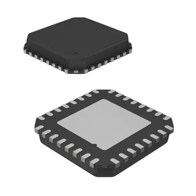
Texas Instruments CC2511F32RSPR
- Part No.:
- CC2511F32RSPR
- Manufacturer:
- Texas Instruments
- Category:
- RF Transceiver ICs
- Package:
- 36-VFQFN Exposed Pad
- Datasheet:
-
 CC2511F32RSPR.pdf
- Description:
- IC RF TXRX+MCU ISM>1GHZ 36VQFN
- Quantity:
- Payment:

- Shipping:

Inventory:1,655
Please send an inquiry. Send us your inquiry, and we will respond immediately.
Product details
Overview
CC2511F32RSPR from Texas Instruments is a low-power 2.4 GHz system-on-chip (SoC) integrating an enhanced 8051 MCU, 32 kB flash, 4 kB RAM, a CC2500-based RF transceiver, and a full-speed USB 2.0 controller - enabling USB dongle designs with −103 dBm sensitivity, 500 kBaud programmable data rate, and 0.3 µA PM3 sleep current.
For engineers reviewing the CC2511F32RSPR datasheet, CC2511F32RSPR pinout, CC2511F32RSPR application, or CC2511F32RSPR equivalent, key selection considerations include USB endpoint configuration (5 bidirectional + control), I2S audio interface support, hardware AES-128 coprocessor, 19 GPIOs, and compliance with FCC Part 15, EN 300 328, and ARIB STD-T-66.
Technical Context
The CC2511F32RSPR implements a dual-oscillator architecture: a 48 MHz crystal oscillator for USB and radio operation, and a low-power RC or 32.768 kHz crystal for sleep timing. Its RF baseband includes hardware-accelerated packet handling with sync word detection, address filtering, automatic CRC, and LQI/RSSI reporting.
MCU subsystem features two data pointers, in-circuit debug via two-wire serial interface, and DMA-driven peripheral transfers - supporting concurrent USB bulk transfers, RF packet RX/TX, and ADC sampling without CPU intervention. Power management supports four modes, with PM3 requiring external interrupt wake-up only.
Key Specifications
| Parameter | Value and Actual Design Meaning |
|---|---|
| RF Frequency Range | 2400–2483.5 MHz ISM band; supports FCC/ETSI/ARIB regulatory compliance |
| Receiver Sensitivity | −103 dBm at 2.4 kBaud; enables robust link budget in low-power remote control applications |
| USB Interface | Full-Speed (12 Mbps); 5 bidirectional endpoints + EP0; 1 kB FIFO; supports bulk/interrupt/isochronous transfers |
| MCU Core | Enhanced 8051; ~8× performance vs standard 8051; two data pointers; hardware debug support |
| Memory | 32 kB in-system programmable flash; 4 kB SRAM; flash endurance ≥1000 write/erase cycles |
| Power Modes | PM3 draws 0.3 µA; wake-up latency 100 µs; requires external interrupt - no RTC or timer wake-up |
| Crypto Engine | Hardware AES-128 coprocessor; supports CCM, CBC-MAC, and ECB modes for secure over-the-air updates |
| Analog Peripherals | 7–12-bit ADC with up to six inputs; I2S interface for stereo digital audio streaming to external DAC/ADC |
Pinout & Package
CC2511F32RSPR uses a 6 × 6 mm QFN-36 package (RoHS-compliant, green, no antimony/bromine) with exposed thermal pad. Pin functions are validated per SWRS055G Rev G, Section 7.
| Pin/Terminal | Circuit Role | Design Meaning |
|---|---|---|
| VDD | Supply voltage input | 3.0–3.6 V main power rail; requires local 100 nF + 1 µF decoupling per supply pin |
| GND | Ground reference | Multiple dedicated GND pins; must connect to solid ground plane for RF stability |
| RF_P / RF_N | Differential RF transceiver interface | 50 Ω differential output; requires balun and impedance-matched PCB trace routing |
| USB_DP / USB_DM | Full-Speed USB differential pair | Requires 90 Ω differential impedance; series 27 Ω resistors recommended near PHY |
| XOSC_Q1 / XOSC_Q2 | 48 MHz crystal oscillator terminals | Must use fundamental-mode 48 MHz crystal; load capacitance 12 pF typical |
| P0_0–P0_7 | Port 0 GPIO | Eight configurable digital I/O; P0_0–P0_2 support USART0; P0_3–P0_4 support I2S |
| P1_0–P1_7 | Port 1 GPIO | Eight configurable digital I/O; P1_0–P1_1 support USART1; P1_2–P1_3 support ADC |
| P2_0–P2_2 | Port 2 GPIO | Three configurable digital I/O; P2_0 supports USB suspend; P2_1/P2_2 support debug interface |
Key Features
| Feature | Design Value |
|---|---|
| Integrated USB 2.0 FS Controller | Eliminates external USB bridge IC; reduces BOM count and PCB area in dongle designs |
| Hardware AES-128 Coprocessor | Offloads encryption/decryption from CPU; enables secure firmware updates without software overhead |
| I2S Audio Interface | Supports mono/stereo PCM at configurable sample rates; directly interfaces with audio codecs for voice-quality wireless audio |
| CC2500-Based RF Transceiver | Delivers proven RF performance: −103 dBm sensitivity, 500 kBaud max data rate, and integrated packet handler |
| DMA-Driven Peripherals | Enables zero-CPU-overhead USB ↔ RF data forwarding and ADC → RAM transfers in low-duty-cycle telemetry |
| Four Power Modes with Sub-µA Sleep | PM3 (0.3 µA) extends battery life in remote controls and sports sensors where wake events are infrequent |
Applications
| Wireless USB Dongles | Wireless Voice-Quality Audio |
|---|---|
Use Scenario: Plug-and-play 2.4 GHz USB adapter for legacy HID devices (keyboards, mice, gamepads) on modern PCs. IC Role / Device Role / Timing Role: SoC acts as USB device endpoint with embedded RF transceiver; handles HID report parsing, RF packet assembly, and USB enumeration. Use Value: Full-speed USB (12 Mbps) prevents bottlenecks seen with RS-232 or low-speed USB; 32 kB flash stores HID descriptor and protocol stack. | Use Scenario: Low-latency stereo audio streaming from PC/mobile to wireless headphones or speaker systems. IC Role / Device Role / Timing Role: I2S master driving external DAC; RF transceiver manages time-synchronized packet delivery with LQI-based retransmission. Use Value: Hardware I2S + 500 kBaud RF supports CD-quality (44.1 kHz/16-bit) audio with <20 ms end-to-end latency. |
| RF-Enabled Remote Controls | Low-Power Telemetry Sensors |
Use Scenario: Battery-powered TV/media remotes transmitting encrypted commands over 2.4 GHz ISM band. IC Role / Device Role / Timing Role: MCU executes button scan logic; RF transceiver sends short burst packets; USB not used - powered from coin cell. Use Value: 0.3 µA PM3 current enables >2-year battery life; AES coprocessor secures command payloads against replay attacks. | Use Scenario: Wireless environmental sensor node (temperature/humidity) reporting to gateway every 5 minutes. IC Role / Device Role / Timing Role: ADC samples sensor; DMA moves data to RAM; RF transmits encrypted packet; enters PM3 between transmissions. Use Value: Integrated ADC + RF + low-power modes eliminate discrete signal chain components; single-chip solution reduces size and power. |
Equivalent & Alternatives
The following parts are listed as comparable options for similar 2.4 GHz SoC with USB applications.
| Alternative Part | Technical Difference | Application Difference | Selection Advice |
|---|---|---|---|
| CC2511F16RSPR | 16 kB flash, 2 kB RAM; identical USB/RF/peripheral set and pinout | Suitable for simpler HID protocols with smaller firmware footprint | Select when firmware size ≤14 kB and memory headroom is not required |
| CC2531F256RHAR | Zigbee-certified SoC; 256 kB flash; no USB controller; 2.4 GHz RF only; different pinout and package (QFN-40) | Targets mesh network coordinator/end-device roles, not USB dongles | Choose only for Zigbee-compliant systems requiring IEEE 802.15.4 MAC/PHY and no host USB interface |
Compared with CC2511F16RSPR, CC2511F32RSPR provides 16 kB additional flash for complex protocol stacks or OTA update partitions; compared with CC2531F256RHAR, it trades Zigbee certification and larger memory for integrated USB 2.0 - eliminating bridge ICs and simplifying dongle BOMs.
Availability
CC2511F32RSPR is available at Aetrix Electronics and suitable for wireless USB dongles, voice-quality audio adapters, RF remote controls, and low-power telemetry sensors requiring stable component supply across industrial and consumer production programs.
Supply support for CC2511F32RSPR includes scheduled delivery planning, volume procurement assistance, BOM continuity management, traceable sourcing, and lifecycle availability coordination for OEM customers, industrial embedded developers, connected-device designers, and electronics production programs.
Manufacturer
Texas Instruments is a global semiconductor leader delivering analog, embedded processing, and connectivity solutions for industrial, automotive, and personal electronics markets.
The CC2511Fx product line targets cost-sensitive, battery-operated 2.4 GHz wireless applications - specifically designed to integrate MCU, RF, USB, and security into a single chip for USB dongles and audio peripherals.
FAQ
What is the maximum data rate supported by the CC2511F32RSPR RF transceiver?
The CC2511F32RSPR RF transceiver supports a programmable data rate up to 500 kBaud using (shaped) MSK modulation. At 2.4 kBaud, it achieves −103 dBm receiver sensitivity. GFSK and 2-FSK are also supported, with data rates ranging from 1.2 to 250 kBaud depending on modulation and filtering configuration. The CC2511F32RSPR does not support Bluetooth or proprietary high-throughput protocols beyond its specified RF baseband capabilities.
Does the CC2511F32RSPR support USB device enumeration without external components?
Yes, the CC2511F32RSPR integrates a full-speed USB 2.0 controller with on-die transceiver, enabling direct USB device enumeration without external PHY or level-shifting components. It supports control, bulk, interrupt, and isochronous transfer types, with 1 kB of dedicated endpoint FIFO memory. The CC2511F32RSPR requires only a 48 MHz crystal, USB_DP/DM termination resistors, and proper ESD protection - no external USB bridge IC is needed.
How many GPIO pins does the CC2511F32RSPR provide, and which ports are available?
The CC2511F32RSPR provides 19 configurable general-purpose digital I/O pins across three ports: Port 0 (P0_0–P0_7, 8 pins), Port 1 (P1_0–P1_7, 8 pins), and Port 2 (P2_0–P2_2, 3 pins). Unlike the CC2510Fx variant, the CC2511F32RSPR excludes P2_3–P2_4, resulting in 19 total GPIOs. Each pin supports multiple peripheral functions including USART, I2S, ADC, and debug interface, configurable via register settings.
What power supply requirements must be met for reliable operation of the CC2511F32RSPR?
The CC2511F32RSPR requires a regulated 3.0–3.6 V supply on all VDD pins, with separate decoupling for digital, analog, and RF domains. Per SWRS055G, each VDD pin needs a 100 nF ceramic capacitor plus a 1 µF bulk capacitor. The RF section demands tight layout isolation and a solid ground plane beneath the QFN-36 thermal pad. Supply voltage below 3.0 V disables USB functionality and may cause RF instability; operation above 3.6 V risks permanent damage per absolute maximum ratings.
Is the CC2511F32RSPR compatible with the CC2510Fx family in terms of firmware and toolchain?
Firmware for the CC2511F32RSPR is source-compatible with CC2510Fx variants at the 8051 instruction level and peripheral register map, but not binary-compatible due to USB controller presence and differing clock tree (48 MHz vs 24–27 MHz). IAR Embedded Workbench and TI's SmartRF Studio support both families, though CC2511F32RSPR projects require USB stack integration and updated startup code for 48 MHz crystal initialization - the CC2511F32RSPR cannot run unmodified CC2510Fx firmware.
CC2511F32RSPR Specifications
- Product attributes
- Attribute value
- Manufacturer:
- Texas Instruments
- Series:
- -
- Package/Case:
- 36-VFQFN Exposed Pad
- Packaging:
- Tape & Reel (TR)
- Product Status:
- Active
- Programmable:
- Not Verified
- Type:
- TxRx + MCU
- RF Family/Standard:
- General ISM > 1GHz
- Protocol:
- -
- Modulation:
- 2FSK, GFSK, MSK
- Frequency:
- 2.4GHz
- Data Rate (Max):
- 500kBaud
- Power - Output:
- 1dBm
- Sensitivity:
- -103dBm
- Memory Size:
- 32kB Flash, 4kB SRAM
- Serial Interfaces:
- I2S, SPI, USART, USB
- GPIO:
- 19
- Voltage - Supply:
- 3V ~ 3.6V
- Current - Receiving:
- 14.7mA ~ 22.9mA
- Current - Transmitting:
- 15.5mA ~ 26mA
- Operating Temperature:
- 0°C ~ 85°C
- Grade:
- -
- Qualification:
- -
- Supplier Device Package:
- 36-VQFN (6x6)
CC2511F32RSPR FAQ
1.How can I place an order for CC2511F32RSPR through Aetrix?
Please submit a Request for Quotation (RFQ) for CC2511F32RSPR on Aetrix. Our sales agent will provide a competitive quotation and guide you through the order confirmation once you accept the terms.
2.Are the price and stock information for CC2511F32RSPR reliable?
The price and inventory of CC2511F32RSPR are updated periodically and may fluctuate due to market conditions. Stock and pricing data are typically refreshed every 24 hours. Quotation validity for CC2511F32RSPR is usually 5 days.
3.What payment methods are accepted for CC2511F32RSPR?
We accept Wire Transfer, PayPal, Credit Card, Western Union, MoneyGram, and Escrow for CC2511F32RSPR transactions.
Note: Certain payment methods may incur a processing fee.
4.How is shipping managed for CC2511F32RSPR?
CC2511F32RSPR orders can be shipped via leading logistics carriers, including DHL, UPS, FedEx, TNT, or Registered Mail.
Once your CC2511F32RSPR order is processed, you will receive an email with the shipment details and tracking number.
Note: Tracking information may take up to 24 hours to appear. Express delivery typically takes 3–5 business days.
5.How can I obtain technical support or documentation for CC2511F32RSPR?
For technical support, including CC2511F32RSPR datasheets, pinout diagrams, or application guidance, please contact our engineering support team. They can provide detailed documentation and assistance for your CC2511F32RSPR requirements.
6.How does Aetrix verify that CC2511F32RSPR is sourced from the original manufacturer or authorized distributors?
All CC2511F32RSPR products on Aetrix are procured from qualified distributors and authorized channels. Our dedicated quality assurance team conducts strict verification, including traceability checks and, if necessary, third-party testing. This ensures that CC2511F32RSPR meets industry standards.
7.What is the process for return or replacement of CC2511F32RSPR?
All CC2511F32RSPR units undergo pre-shipment inspection (PSI). If there is an issue with CC2511F32RSPR, returns or replacements are accepted under the following conditions:
1.Quantity discrepancies, incorrect items, or visible external defects (such as breakage or corrosion), acknowledged by Aetrix.
2.The issue is reported within 90 days of delivery.
3.The CC2511F32RSPR part is unused and in its original packaging.
Return procedure for CC2511F32RSPR:
1.Submit a request within 90 days.
2.Obtain a Return Material Authorization (RMA) from Aetrix.
CC2511F32RSPR Tags

-
ESP32-D0WD-V3
Espressif Systems

-
ESP8266EX
Espressif Systems

-
ESP32-S3
Espressif Systems

-
NRF24L01P-R7
Nordic Semiconductor ASA
-
NRF24L01P-R
Nordic Semiconductor ASA

-
ESP32-U4WDH
Espressif Systems

-
DA14531-00000OG2
Renesas
-
ESP32-C6FH4
Espressif Systems

-
DA14531-00000FX2
Renesas
-
NRF24L01P-T
Nordic Semiconductor ASA

-
NRF52810-QCAA-R
Nordic Semiconductor ASA
-
ESP32-S3FN8
Espressif Systems
Tech Hub

A practical engineering guide to 3.3V and 5V logic compatibility, input thresholds, resistor dividers, translator ICs, MOSFET level shifting, I2C pull-ups, timing limits and power-sequencing risks.

The 74HC595 uses push-pull logic outputs, while the TPIC6B595 uses 50 V open-drain DMOS sinks for higher-power loads. This guide compares timing, current limits, 3.3 V interfacing, load wiring, thermal…

The 74HC595 converts serial data into eight stable parallel outputs. This guide covers pin functions, shift and storage timing, OE and MR behavior, drive-current limits, cascading, voltage compatibilit…

A technical comparison of level-sensitive latches and edge-triggered flip-flops, covering timing windows, setup and hold limits, master–slave operation, time borrowing, race-through, HDL inference and…

A D latch stores one bit while Enable controls when data can pass. This reference covers gate-level operation, truth tables, transparency, setup and hold timing, LE versus OE, common ICs and practical …

An SR latch stores one bit through cross-coupled feedback. This engineering reference covers NOR and NAND implementations, truth tables, forbidden-state recovery, gated operation, switch debouncing, fa…

Latch circuits retain one bit through feedback. This technical reference covers SR and D latches, truth tables, transparency, timing limits, latch-versus-flip-flop behavior, applications and common log…

An engineering guide to LED driver operation, constant-current and constant-voltage outputs, linear and switching topologies, dimming, IC selection, calculations, replacement compatibility, and fault c…

Operational amplifier guide covering op amp basics, feedback, ideal vs real op amps, common configurations, buffer circuits, offset, bias current, gain-bandwidth, slew rate, rail-to-rail limits and sel…

Jumper cables guide covering safe connection order, red and black clamp placement, final ground connection, cable gauge, length, clamp quality, copper vs CCA cables, jump starter comparison and battery…


