
 My Inquiry
 My Account


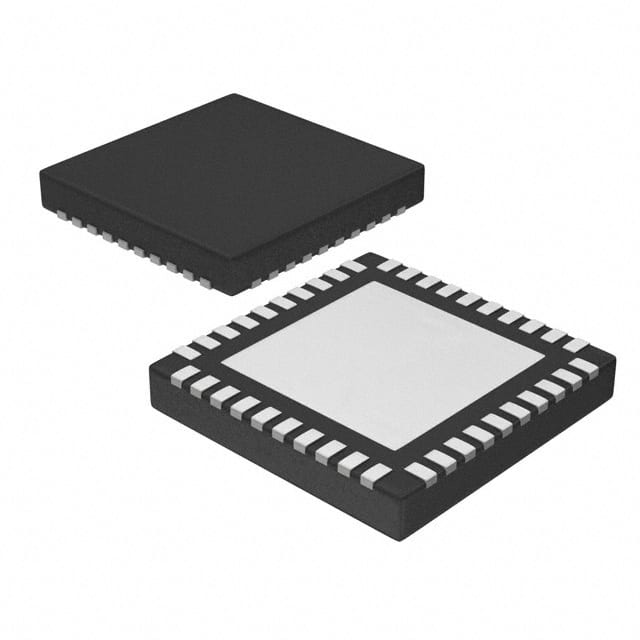
Texas Instruments CDCU877RHAT
- Part No.:
- CDCU877RHAT
- Manufacturer:
- Texas Instruments
- Category:
- Application Specific Clock/Timing
- Package:
- 40-VFQFN Exposed Pad
- Datasheet:
-
 CDCU877RHAT.pdf
- Description:
- IC PLL CLOCK DRIVER 1.8V 40VQFN
- Quantity:
- Payment:

- Shipping:

Inventory:2,546
Please send an inquiry. Send us your inquiry, and we will respond immediately.
Product details
Overview
CDCU877RHAT from Texas Instruments is a 1.8-V phase-locked loop (PLL) clock driver IC designed for DDR II memory subsystems. It distributes one differential clock input (CK/CK) to ten differential output pairs (Y0–Y9/Y0–Y9) and one feedback pair (FBOUT/FBOUT), with ±50 ps static phase offset, 35 ps output skew, and operation from 10 MHz to 400 MHz. It supports spread-spectrum clocking and operates across –40°C to 85°C.
For engineers reviewing the CDCU877RHAT datasheet, CDCU877RHAT pinout, CDCU877RHAT application, or CDCU877RHAT equivalent, key selection criteria include its 40-pin VQFN (RHA) package, low-jitter performance (±30 ps cycle-to-cycle), fail-safe inputs, OE/OS control logic, and compliance with JESD82-8 for PC2-3200/4300 DDR2 DIMMs.
Technical Context
The CDCU877RHAT implements a zero-delay PLL architecture that synchronizes outputs to the input clock via external feedback pins (FBIN/FBIN), enabling precise phase alignment in high-speed DDR2 memory interfaces. Its internal analog PLL remains active during OE-low states-except for Y7/Y7, which remain free-running when OS and OE are both low.
It features dual power domains: AVDD powers the analog PLL core (bypassable by grounding), while VDDQ supplies digital I/O and outputs. Input logic detection enables automatic low-power mode when CK/CK are held logic-low, turning off outputs, feedback, and PLL without external control.
Key Specifications
| Parameter | Value and Actual Design Meaning |
|---|---|
| Operating Frequency | 10 MHz to 400 MHz - supports full DDR2 clock range including 200–340 MHz application band with guaranteed timing compliance. |
| Static Phase Offset | ±50 ps - ensures minimal deterministic timing error between input and synchronized outputs for tight setup/hold margins. |
| Output Skew | 35 ps - guarantees matched propagation delay across all ten Y/Y output pairs, critical for parallel DDR2 data strobes. |
| Cycle-Cycle Jitter | ±30 ps - measured at 160–340 MHz; enables robust timing margin in high-speed DDR2 write leveling and read capture. |
| Supply Voltage | VDDQ = 1.7–1.9 V, AVDD = same as VDDQ - requires tightly regulated 1.8-V rail; AVDD grounding disables PLL for test mode. |
| Power Consumption | <135 mA dynamic current at 270 MHz - enables thermal management in dense memory modules with multiple clock buffers. |
| Temperature Range | –40°C to +85°C - qualified for industrial-grade DDR2 server and telecom memory applications. |
Pinout & Package
The CDCU877RHAT uses a 40-pin VQFN (RHA) package, 6.0 mm × 6.0 mm body, 0.5 mm pitch, with exposed thermal pad (Pin 41) requiring PCB solder connection for thermal and mechanical integrity.
| Pin/Terminal | Circuit Role | Design Meaning |
|---|---|---|
| CK / CK | Differential clock input | LVDS-compatible inputs with 10 kΩ pulldown resistors; detect logic-low state independently to trigger auto-power-down. |
| FBIN / FBIN | Differential feedback input | Connects to FBOUT/FBOUT to close PLL loop; determines output phase lock point and jitter transfer function. |
| FBOUT / FBOUT | Differential feedback output | Provides buffered copy of internal feedback path; used externally to stabilize PLL against board trace delays. |
| OE | Asynchronous output enable | Active-low; disables all Y/Y outputs except Y7/Y7 when OS = low; PLL remains locked and functional. |
| OS | Output select configuration | Must be hard-wired to GND or VDD; selects OE behavior mode and determines whether Y7/Y7 are always enabled. |
| VDDQ (Pins 1,6,9,15,20,23,28,31,36) | Digital/output power supply | Nine dedicated VDDQ pins minimize IR drop and supply noise on high-speed clock outputs. |
| GND (Pins 2,12,13,18,17,30,32,35,37,40) | Ground reference | Ten GND pins provide low-inductance return paths for clock outputs and reduce ground bounce in multi-output switching. |
| Y[0:9] / Y[0:9] | Differential clock outputs | 10 fully buffered LVDS-like outputs; each pair drives one DDR2 memory rank or register; no internal termination required. |
| AVDD / AGND | Analog PLL power/ground | Separate analog domain isolates PLL core from digital noise; requires dedicated LC filtering per Figure 12. |
Key Features
| Feature | Design Value |
|---|---|
| Spread-spectrum clock (SSC) tracking | Supports 30–33 kHz modulation with ≤0.5% frequency deviation-reduces EMI peak emissions in memory subsystems without degrading timing margins. |
| Fail-safe input detection | Independent logic-level detector on CK/CK inputs enables automatic entry into low-power mode when clocks stop-no external controller needed. |
| Configurable Y7/Y7 output behavior | When OS = low and OE = low, Y7/Y7 remain active while other outputs disable-enables partial system wake-up or debug clock routing. |
| Test-mode PLL bypass | Grounding AVDD disables and bypasses PLL while preserving VDDQ functionality-allows functional testing of output buffers without PLL lock dependency. |
| JESD82-8 compliance | Meets or exceeds JEDEC standard for PC2-3200/4300 DDR2 clock drivers-ensures interoperability with industry-standard DDR2 memory modules. |
Applications
| DDR2 Memory Module Clock Distribution | Server Memory Subsystem Timing |
|---|---|
Use Scenario: Driving clock signals to multiple DDR2 SDRAM chips on a UDIMM or RDIMM module. IC Role / Device Role / Timing Role: Zero-delay PLL clock buffer distributing one reference clock to ten output pairs with matched skew and low jitter. Use Value: Enables simultaneous clocking of up to ten memory ranks with <35 ps inter-output skew, meeting JEDEC tSKO requirements for PC2-3200/4300. | Use Scenario: Providing synchronized clocks to memory controllers, registers, and data buffers in dual-processor server motherboards. IC Role / Device Role / Timing Role: High-stability clock distribution hub with SSC compatibility and fail-safe power-down for thermal-aware memory management. Use Value: Reduces EMI by >10 dB through SSC tracking while maintaining ±30 ps cycle-cycle jitter-critical for PCIe-adjacent memory layouts. |
| Industrial DDR2-Based Control Systems | Telecom Baseband Memory Interfaces |
Use Scenario: Clocking DDR2 memory in programmable logic controllers (PLCs) operating in extended temperature environments. IC Role / Device Role / Timing Role: Industrial-grade clock driver with –40°C to +85°C operation and robust input detection for unattended systems. Use Value: Auto-power-down on clock loss prevents spurious output transitions during brown-out or cable disconnect events-improves system reliability. | Use Scenario: Timing interface between FPGA-based baseband processors and DDR2 memory in wireless infrastructure equipment. IC Role / Device Role / Timing Role: Low-jitter, low-skew clock repeater supporting 266–333 MHz DDR2 data rates with programmable OE/OS control. Use Value: Configurable Y7/Y7 output allows independent clocking of FPGA configuration memory during runtime reconfiguration sequences. |
Equivalent & Alternatives
The following parts are listed as comparable options for similar PLL clock driver applications.
| Alternative Part | Technical Difference | Application Difference | Selection Advice |
|---|---|---|---|
| IDT8T49N242A | 2.5-V/3.3-V supply; integrated crystal oscillator; higher integration but no SSC support. | Targeted at telecom sync applications with Stratum-3 timing; not optimized for DDR2 DIMM form factor or JEDEC compliance. | Choose when needing built-in XO and lower phase noise at 122.88 MHz; avoid for DDR2 memory modules requiring 1.8-V operation and SSC tracking. |
| ICS85310AMLF | 3.3-V LVPECL outputs; no AVDD/VDDQ separation; fixed 1:10 fanout without feedback option. | Designed for general-purpose clock distribution in backplanes and FPGAs-not validated for DDR2 memory timing standards. | Choose for non-DDR2 systems needing LVPECL levels and simpler pinout; avoid where JESD82-8 compliance, 1.8-V operation, or PLL-based skew correction is required. |
Compared with IDT8T49N242A and ICS85310AMLF, the CDCU877RHAT uniquely combines 1.8-V operation, external feedback PLL architecture, SSC tracking, and JEDEC DDR2 compliance-making it the only suitable choice for cost-sensitive, standards-conforming DDR2 memory clocking in industrial and server platforms.
Availability
CDCU877RHAT is available at Aetrix Electronics and suitable for DDR2 memory modules, server motherboard designs, and industrial control systems requiring stable component supply, long-term lifecycle support, and RoHS-compliant packaging.
Supply support for CDCU877RHAT includes scheduled delivery planning, volume procurement assistance, BOM continuity management, traceable sourcing, and lifecycle availability coordination for OEM customers, industrial embedded developers, connected-device designers, and electronics production programs.
Manufacturer
Texas Instruments is a global semiconductor leader specializing in analog, embedded processing, and clock solutions, with decades of expertise in high-performance timing devices for memory and computing systems.
The CDCU877RHAT belongs to TI's DDR2 clock buffer product line, engineered specifically to meet JEDEC JESD82-8 requirements for PC2-3200/4300 memory interfaces-emphasizing low skew, SSC compatibility, and industrial temperature operation.
FAQ
What is the recommended power supply decoupling for CDCU877RHAT?
CDCU877RHAT requires separate decoupling for AVDD and VDDQ. For AVDD, TI recommends a 4.7-μF bead-filtered network with 0.1-μF and 2200-pF capacitors placed close to the device (Figure 12). VDDQ pins must each have ≥0.1-μF ceramic capacitance near the pin. All GND connections must tie to a solid analog/digital split plane with low-inductance vias. This ensures PLL stability and minimizes output jitter in CDCU877RHAT.
Does CDCU877RHAT support pin-compatible replacement with CDCU877ARHAT?
No, CDCU877RHAT and CDCU877ARHAT are not pin-compatible replacements. While both use the RHA 40-pin VQFN package, CDCU877ARHAT is the A-version with lower output cross-voltage (VOX) and tighter VOX tolerance (±30 mV vs. CDCU877RHAT's unspecified VOX). Electrical behavior differs in dynamic phase offset and SSC response-TI does not guarantee interchangeability. Always verify layout and timing against the correct datasheet revision for CDCU877RHAT.
How does the OS pin affect CDCU877RHAT output behavior?
The OS pin on CDCU877RHAT configures OE functionality: when OS = high, OE operates as standard asynchronous output enable; when OS = low and OE = low, Y7/Y7 remain active while all other Y/Y outputs disable. This allows selective clock gating-e.g., keeping one memory rank active during partial system sleep. OS must be hard-wired to GND or VDD; floating OS causes undefined behavior in CDCU877RHAT.
Can CDCU877RHAT operate without external feedback (FBIN/FBIN)?
No, CDCU877RHAT requires external feedback via FBIN/FBIN to maintain PLL lock and achieve zero-delay operation. If FBIN/FBIN are left unconnected or tied incorrectly, the PLL fails to lock, resulting in high jitter, phase drift, or disabled outputs. The feedback path must connect FBOUT/FBOUT to FBIN/FBIN with matched trace lengths. Open-loop operation is not supported in CDCU877RHAT.
What is the stabilization time for CDCU877RHAT after power-up or clock resume?
The CDCU877RHAT stabilization time-the duration required to achieve PLL phase lock-is 12 μs maximum, measured from power-on or from logic-low clock recovery (per datasheet Section 6.3). This applies under AVDD = VDDQ = 1.8 V, TA = 25°C, and with properly terminated FBIN/FBIN. Stabilization time remains consistent across the full –40°C to +85°C range and is unaffected by OE/OS state-critical for DDR2 initialization sequences in CDCU877RHAT.
CDCU877RHAT Specifications
- Product attributes
- Attribute value
- Manufacturer:
- Texas Instruments
- Series:
- -
- Package/Case:
- 40-VFQFN Exposed Pad
- Packaging:
- Tape & Reel (TR)
- Product Status:
- Active
- Programmable:
- Not Verified
- PLL:
- Yes
- Main Purpose:
- Memory, DDR2
- Input:
- SSTL-18
- Output:
- SSTL-18
- Number of Circuits:
- 1
- Ratio - Input:Output:
- 1:10
- Differential - Input:Output:
- Yes/Yes
- Frequency - Max:
- 400MHz
- Voltage - Supply:
- 1.7V ~ 1.9V
- Operating Temperature:
- -40°C ~ 85°C
- Mounting Type:
- Surface Mount
- Grade:
- -
- Qualification:
- -
- Supplier Device Package:
- 40-VQFN (6x6)
CDCU877RHAT FAQ
1.How can I place an order for CDCU877RHAT through Aetrix?
Please submit a Request for Quotation (RFQ) for CDCU877RHAT on Aetrix. Our sales agent will provide a competitive quotation and guide you through the order confirmation once you accept the terms.
2.Are the price and stock information for CDCU877RHAT reliable?
The price and inventory of CDCU877RHAT are updated periodically and may fluctuate due to market conditions. Stock and pricing data are typically refreshed every 24 hours. Quotation validity for CDCU877RHAT is usually 5 days.
3.What payment methods are accepted for CDCU877RHAT?
We accept Wire Transfer, PayPal, Credit Card, Western Union, MoneyGram, and Escrow for CDCU877RHAT transactions.
Note: Certain payment methods may incur a processing fee.
4.How is shipping managed for CDCU877RHAT?
CDCU877RHAT orders can be shipped via leading logistics carriers, including DHL, UPS, FedEx, TNT, or Registered Mail.
Once your CDCU877RHAT order is processed, you will receive an email with the shipment details and tracking number.
Note: Tracking information may take up to 24 hours to appear. Express delivery typically takes 3–5 business days.
5.How can I obtain technical support or documentation for CDCU877RHAT?
For technical support, including CDCU877RHAT datasheets, pinout diagrams, or application guidance, please contact our engineering support team. They can provide detailed documentation and assistance for your CDCU877RHAT requirements.
6.How does Aetrix verify that CDCU877RHAT is sourced from the original manufacturer or authorized distributors?
All CDCU877RHAT products on Aetrix are procured from qualified distributors and authorized channels. Our dedicated quality assurance team conducts strict verification, including traceability checks and, if necessary, third-party testing. This ensures that CDCU877RHAT meets industry standards.
7.What is the process for return or replacement of CDCU877RHAT?
All CDCU877RHAT units undergo pre-shipment inspection (PSI). If there is an issue with CDCU877RHAT, returns or replacements are accepted under the following conditions:
1.Quantity discrepancies, incorrect items, or visible external defects (such as breakage or corrosion), acknowledged by Aetrix.
2.The issue is reported within 90 days of delivery.
3.The CDCU877RHAT part is unused and in its original packaging.
Return procedure for CDCU877RHAT:
1.Submit a request within 90 days.
2.Obtain a Return Material Authorization (RMA) from Aetrix.
CDCU877RHAT Tags
-
LMK00334RTVRQ1
Texas Instruments
.jpg)
-
DSC557-0344FI0T
Microchip Technology
-
9FGV0241AKILFT
Renesas

-
9DBL0452CKILFT
Renesas
-
DSC557-0344FL1T
Microchip Technology
-
RC19008AGND#KB0
Renesas
-
RC19008AGND#BB0
Renesas

-
9DB403DGILFT
Renesas
-
9DB233AGILFT
Renesas

-
9DB803DGILFT
Renesas
-
9FGL0851DKILFT
Renesas
-
AB-557-03-HCHC-F-L-C-T
Abracon LLC
Tech Hub

A practical engineering guide to 3.3V and 5V logic compatibility, input thresholds, resistor dividers, translator ICs, MOSFET level shifting, I2C pull-ups, timing limits and power-sequencing risks.

The 74HC595 uses push-pull logic outputs, while the TPIC6B595 uses 50 V open-drain DMOS sinks for higher-power loads. This guide compares timing, current limits, 3.3 V interfacing, load wiring, thermal…

The 74HC595 converts serial data into eight stable parallel outputs. This guide covers pin functions, shift and storage timing, OE and MR behavior, drive-current limits, cascading, voltage compatibilit…

A technical comparison of level-sensitive latches and edge-triggered flip-flops, covering timing windows, setup and hold limits, master–slave operation, time borrowing, race-through, HDL inference and…

A D latch stores one bit while Enable controls when data can pass. This reference covers gate-level operation, truth tables, transparency, setup and hold timing, LE versus OE, common ICs and practical …

An SR latch stores one bit through cross-coupled feedback. This engineering reference covers NOR and NAND implementations, truth tables, forbidden-state recovery, gated operation, switch debouncing, fa…

Latch circuits retain one bit through feedback. This technical reference covers SR and D latches, truth tables, transparency, timing limits, latch-versus-flip-flop behavior, applications and common log…

An engineering guide to LED driver operation, constant-current and constant-voltage outputs, linear and switching topologies, dimming, IC selection, calculations, replacement compatibility, and fault c…

Operational amplifier guide covering op amp basics, feedback, ideal vs real op amps, common configurations, buffer circuits, offset, bias current, gain-bandwidth, slew rate, rail-to-rail limits and sel…

Jumper cables guide covering safe connection order, red and black clamp placement, final ground connection, cable gauge, length, clamp quality, copper vs CCA cables, jump starter comparison and battery…


