
 My Inquiry
 My Account


Renesas CDP68HC68T1M296
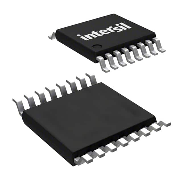
- Part No.:
- CDP68HC68T1M296
- Manufacturer:
- Renesas
- Category:
- Real Time Clocks
- Package:
- 16-SOIC (0.295", 7.50mm Width)
- Datasheet:
-
 CDP68HC68T1M296.pdf
- Description:
- IC RTC CLK/CALENDAR SPI 16SOIC
- Quantity:
- Payment:

- Shipping:

Inventory:4,359
Please send an inquiry. Send us your inquiry, and we will respond immediately.
Product details
Overview
CDP68HC68T1M296 from Intersil is a CMOS serial real-time clock IC with integrated 32×8-bit static RAM, SPI interface, power-sense/control logic, and programmable buffered clock output. It provides BCD-formatted time/calendar (seconds to years), 12/24-hour mode with AM/PM flag, alarm, periodic interrupts, and watchdog reset capability. Used in embedded systems requiring battery-backed timekeeping and intelligent power management.
For engineers reviewing the CDP68HC68T1M296 datasheet, CDP68HC68T1M296 pinout, CDP68HC68T1M296 application, or CDP68HC68T1M296 equivalent, key selection criteria include its 3-wire SPI interface, dual-clock source support (32kHz crystal or 50/60Hz line input), 2.2V minimum standby voltage, three independent interrupt modes (alarm/periodic/power-fail), and CPUR open-drain reset output for processor supervision.
Technical Context
The CDP68HC68T1M296 implements a prescaler-driven 1Hz timebase derived either from an internal oscillator (with 32kHz, 1MHz, 2MHz, or 4MHz crystal) or external 50/60Hz AC line input via the LINE pin. Its clock/calendar registers (addresses $20–$26) and alarm latches ($28–$2A) operate in BCD format and support automatic leap-year correction.
Power control is managed through VSYS/VBATT interaction: VSYS level at end of POR selects single-supply or battery-backup mode; PSE output enables system power rail control; CPUR delivers open-drain reset pulses; and INT provides wired-OR interrupt signaling with status-latched cause (power fail/alarm/periodic). The watchdog requires CE pin toggling without serial transfer to prevent CPU reset.
Key Specifications
| Parameter | Value and Actual Design Meaning |
|---|---|
| Interface | SPI (3-wire: SCK, MOSI, MISO) with CE-controlled chip enable and wired-OR INT output |
| Timekeeping Voltage Range | 2.2V to 6.0V - supports extended battery backup down to 2.2V while maintaining RTC accuracy |
| Crystal Support | 32.768kHz, 1.048576MHz, 2.097152MHz, or 4.194304MHz - selectable via Clock Control Register bits D1–D0 |
| Line Input Compatibility | 50Hz or 60Hz AC signal on LINE pin - enables timekeeping and power-fail detection from mains-derived sources |
| Alarm & Interrupt Modes | Three independent modes: seconds/minutes/hours alarm, 15 programmable periodic intervals (sub-second to daily), and power-fail detect via VSYS/VBATT comparison |
| RAM Capacity | 32 × 8-bit static RAM (addresses $00–$1F) - retains data during VDD loss when VBATT is active |
| Output Flexibility | CLKOUT provides seven selectable frequencies (XTAL, XTAL/2…2Hz, 50/60Hz) or disable; CPUR is open-drain reset; PSE controls external power rail |
Pinout & Package
CDP68HC68T1M296 is packaged in a 16-lead SOIC (Small Outline Integrated Circuit) with Pb-free RoHS-compliant finish (package drawing M16.3), optimized for surface-mount reflow assembly.
| Pin/Terminal | Circuit Role | Design Meaning |
|---|---|---|
| 1 CLKOUT | Programmable clock output | Buffered squarewave output; frequency selected by Clock Control Register (7 options or disable); driven low during power-down |
| 2 CPUR | CPU reset output | Open-drain N-channel output requiring external pull-up; asserts low reset under software watchdog timeout or power-down exit |
| 3 INT | Interrupt output | Wired-OR active-low interrupt signal indicating alarm, periodic event, or power-fail condition; requires external pull-up |
| 4 SCK | SPI clock input | Serial clock input for SPI interface; maximum fSCK = 1 MHz at VDD = 5V |
| 5 MOSI | SPI data input | Master-out/slave-in data line for writing to registers and RAM |
| 6 MISO | SPI data output | Master-in/slave-out data line for reading clock/calendar, status, and RAM contents |
| 7 VSS | Ground reference | Primary ground connection for all internal circuitry and I/O pins |
| 8 CE | Chip enable input | Active-high enable for SPI interface; also serves as watchdog trigger input when toggled without serial transfer |
| 9 VDD | Main supply voltage | Primary power input (3.0–6.0V); powers digital core and I/O; disconnected from oscillator during battery-backup mode |
| 10 XTAL IN | Oscillator input | Input to internal inverter for crystal-based timebase; accepts 32kHz–4MHz crystals or external squarewave clock |
| 11 VBATT | Battery backup supply | Direct connection to backup battery; internally connects to VDD when VSYS falls below VBATT +1.0V |
| 12 VSYS | System voltage sense | Monitors main system supply; determines operating mode (single-supply vs. battery-backup) at POR completion |
| 13 XTAL OUT | Oscillator output | Output from internal inverter; connected to crystal's second terminal in parallel-resonant configuration |
| 14 LINE | AC line input / power sense | Accepts 50/60Hz AC for timekeeping or power-fail detection; must be tied to VDD via 10kΩ if unused |
| 15 POR | Power-on reset input | Schmitt-trigger input accepting external RC network to generate internal reset pulse and initialize registers |
| 16 PSE | Power supply enable output | Open-drain output controlling external power rail; driven high on POR, interrupt, or VSYS recovery; driven low during power-down |
Key Features
| Feature | Design Value |
|---|---|
| Integrated SPI Real-Time Clock + RAM | Single-chip solution combining BCD time/calendar (seconds–years), 32×8-bit nonvolatile RAM, and serial interface - eliminates discrete timing + memory + bus logic |
| Dual Clock Source Selection | Runtime-selectable timebase: crystal (32kHz/1–4MHz) or AC line (50/60Hz) - enables flexible deployment across mains-powered and battery-backed systems |
| Intelligent Power Management | Hardware-assisted power-down with PSE-controlled rail shutdown, CPUR-initiated processor reset, and VSYS/VBATT monitoring - reduces system standby current to µA range |
| Multi-Mode Interrupt Architecture | Three independent, maskable interrupt sources (alarm/periodic/power-fail) with dedicated status bits - simplifies firmware event handling without polling overhead |
| Watchdog Supervision | CE-pin-based watchdog requiring periodic toggle (no serial transfer needed) - detects CPU lockup and triggers CPUR reset without additional components |
| Low-Voltage Timekeeping | Valid operation down to 2.2V on VBATT - extends battery life in backup mode while preserving calendar accuracy and RAM retention |
Applications
| Industrial HMI Panels | Energy Metering Systems |
|---|---|
Use Scenario: Standalone panel with local display, button inputs, and battery-backed logging during mains outage. IC Role / Device Role / Timing Role: Primary RTC and time-stamping engine; maintains accurate wall-clock time and logs events with timestamps during brownouts. Use Value: Enables timestamped fault/event logging even during extended power loss, using VBATT-supplied 2.2V–6.0V timekeeping and 32-byte RAM for buffer storage. |
Use Scenario: DIN-rail mounted electricity meter with tamper detection, tariff switching, and historical consumption storage. IC Role / Device Role / Timing Role: Calendar/time source for tariff scheduling and billing cycles; LINE pin monitors 50Hz grid frequency for synchronization and anomaly detection. Use Value: Uses 50Hz line input for precise timebase and power-fail sensing - eliminates crystal cost and enables grid-synchronized metering without external timing references. |
| Medical Infusion Pumps | Point-of-Sale Terminals |
Use Scenario: Battery-operated infusion device requiring dose logging, runtime tracking, and safety-critical timeout enforcement. IC Role / Device Role / Timing Role: Safety-redundant timekeeper; alarms trigger dose alerts or motor stop; watchdog resets MCU on firmware hang. Use Value: CPUR-driven hardware reset and alarm-triggered INT provide deterministic response to timing faults - critical for ISO 13485 compliance and patient safety. |
Use Scenario: Retail terminal with receipt printing, transaction logging, and offline operation during network outages. IC Role / Device Role / Timing Role: Transaction timestamp generator and offline session timer; RAM stores pending receipts during connectivity loss. Use Value: 32-byte on-chip RAM retains last 10–15 receipts locally; combined with battery-backed RTC, ensures audit trail integrity across power cycles. |
Equivalent & Alternatives
The following parts are listed as comparable options for similar real-time clock with RAM and power management applications.
| Alternative Part | Technical Difference | Application Difference | Selection Advice |
|---|---|---|---|
| DS1307+ (Maxim Integrated) | I²C interface only; no LINE input; no power-sense or CPUR output; 56-byte RAM; no watchdog | Lacks power-fail detection, processor reset, and AC line sync - suitable only for basic timekeeping without system-level power control | Select when SPI is unavailable and advanced power supervision is unnecessary; verify I²C compatibility and external reset circuitry |
| PCF8563 (NXP Semiconductors) | I²C interface; 256-byte RAM; no LINE input; no CPUR or PSE outputs; no watchdog; 1.0–5.5V operation | Higher RAM capacity but missing VSYS/VBATT power-state coordination and hardware reset - requires external supervisor for safe power-down | Choose for higher memory needs and wider voltage range; add discrete reset IC and power controller for full CDP68HC68T1M296 functionality |
Compared with DS1307+ and PCF8563, the CDP68HC68T1M296 uniquely integrates SPI, AC line input, power-sense logic, CPUR reset, and PSE rail control in one package - enabling complete autonomous power management without external supervisors or glue logic.
Availability
CDP68HC68T1M296 is available at Aetrix Electronics and suitable for industrial HMI panels, energy metering systems, medical infusion pumps, and point-of-sale terminals requiring stable component supply with long-term lifecycle support.
Supply support for CDP68HC68T1M296 includes scheduled delivery planning, volume procurement assistance, BOM continuity management, traceable sourcing, and lifecycle availability coordination for OEM customers, industrial embedded developers, connected-device designers, and electronics production programs.
Manufacturer
Intersil (now part of Renesas Electronics) is a semiconductor manufacturer specializing in precision analog, power management, and timing solutions for industrial, automotive, and communications markets.
The CDP68HC68T1 product line was designed for embedded systems needing integrated RTC, nonvolatile RAM, and intelligent power supervision - targeting applications where battery backup, power-fail response, and processor reset coordination are critical.
FAQ
What clock sources does the CDP68HC68T1M296 support?
The CDP68HC68T1M296 supports four crystal frequencies (32.768kHz, 1.048576MHz, 2.097152MHz, 4.194304MHz) selected via the Clock Control Register, or an external 50Hz/60Hz AC signal applied to the LINE pin. Crystal operation is mandatory when power-sense mode is enabled, as the LINE input is disconnected from the prescaler in that configuration. The CDP68HC68T1M296 does not support arbitrary clock frequencies outside these defined options.
How does the CDP68HC68T1M296 handle power failure detection?
The CDP68HC68T1M296 detects power failure using two complementary methods: (1) VSYS/VBATT comparison - when VSYS drops below VBATT +1.0V, the device enters battery-backup mode and asserts PSE low; (2) LINE pin monitoring - with Bit 5 set in the Interrupt Control Register, AC zero-crossing loss on the LINE pin triggers a power-fail interrupt after 2.68–4.64ms delay. Both mechanisms set the Power-sense Interrupt bit in the Status Register and drive INT low. The CDP68HC68T1M296 requires crystal operation for method (2).
Can the CDP68HC68T1M296 operate with only a battery supply?
Yes, the CDP68HC68T1M296 supports true battery-backup operation. When VSYS is low at end-of-POR, it enters battery-backup mode: CLKOUT, CPUR, and PSE are held low until VSYS rises ~1.0V above VBATT. During this state, the oscillator runs from VBATT, timekeeping continues at 2.2–6.0V, and RAM retains data. VDD may be unpowered. The CDP68HC68T1M296 maintains full RTC functionality including alarm and periodic interrupts while drawing only 10–500µA (depending on crystal frequency), making it suitable for multi-year battery operation.
What is the function of the CE pin beyond chip enable?
Beyond enabling the SPI interface, the CE pin serves as the watchdog trigger input. When Bit 7 (Watchdog) is set in the Interrupt Control Register, the CDP68HC68T1M296 requires the host CPU to toggle CE high/low periodically without initiating a serial transfer. Failure to do so within the timeout window causes the CDP68HC68T1M296 to assert CPUR low and set Bit 6 in the Status Register. This provides hardware-enforced CPU supervision independent of SPI traffic - a feature not found in most competing RTCs like DS1307+ or PCF8563.
Does the CDP68HC68T1M296 support both 12-hour and 24-hour time formats?
Yes, the CDP68HC68T1M296 supports both formats. Bit 7 of the Hours register ($22) selects mode: '1' enables 12-hour format with AM/PM indication in Bit 5; '0' selects 24-hour format (00–23). In 12-hour mode, hours are encoded as 01–12 (AM) or 21–32 (PM) in BCD; in 24-hour mode, values are 00–23. The CDP68HC68T1M296 automatically handles rollover and leap-year correction regardless of format, and the selection persists across power cycles when stored in the clock registers.
CDP68HC68T1M296 Specifications
- Product attributes
- Attribute value
- Manufacturer:
- Renesas
- Series:
- -
- Package/Case:
- 16-SOIC (0.295", 7.50mm Width)
- Packaging:
- Tape & Reel (TR)
- Product Status:
- Obsolete
- Programmable:
- Not Verified
- Type:
- Clock/Calendar
- Features:
- Alarm, Leap Year, Square Wave Output, Watchdog Timer
- Memory Size:
- 32B
- Time Format:
- HH:MM:SS (12/24 hr)
- Date Format:
- YY-MM-DD-dd
- Interface:
- SPI
- Voltage - Supply:
- 3V ~ 6V
- Voltage - Supply, Battery:
- 2.2V ~ 6V
- Current - Timekeeping (Max):
- 20µA ~ 500µA @ 5V
- Operating Temperature:
- -40°C ~ 85°C
- Mounting Type:
- Surface Mount
- Grade:
- -
- Qualification:
- -
- Supplier Device Package:
- 16-SOIC
CDP68HC68T1M296 FAQ
1.How can I place an order for CDP68HC68T1M296 through Aetrix?
Please submit a Request for Quotation (RFQ) for CDP68HC68T1M296 on Aetrix. Our sales agent will provide a competitive quotation and guide you through the order confirmation once you accept the terms.
2.Are the price and stock information for CDP68HC68T1M296 reliable?
The price and inventory of CDP68HC68T1M296 are updated periodically and may fluctuate due to market conditions. Stock and pricing data are typically refreshed every 24 hours. Quotation validity for CDP68HC68T1M296 is usually 5 days.
3.What payment methods are accepted for CDP68HC68T1M296?
We accept Wire Transfer, PayPal, Credit Card, Western Union, MoneyGram, and Escrow for CDP68HC68T1M296 transactions.
Note: Certain payment methods may incur a processing fee.
4.How is shipping managed for CDP68HC68T1M296?
CDP68HC68T1M296 orders can be shipped via leading logistics carriers, including DHL, UPS, FedEx, TNT, or Registered Mail.
Once your CDP68HC68T1M296 order is processed, you will receive an email with the shipment details and tracking number.
Note: Tracking information may take up to 24 hours to appear. Express delivery typically takes 3–5 business days.
5.How can I obtain technical support or documentation for CDP68HC68T1M296?
For technical support, including CDP68HC68T1M296 datasheets, pinout diagrams, or application guidance, please contact our engineering support team. They can provide detailed documentation and assistance for your CDP68HC68T1M296 requirements.
6.How does Aetrix verify that CDP68HC68T1M296 is sourced from the original manufacturer or authorized distributors?
All CDP68HC68T1M296 products on Aetrix are procured from qualified distributors and authorized channels. Our dedicated quality assurance team conducts strict verification, including traceability checks and, if necessary, third-party testing. This ensures that CDP68HC68T1M296 meets industry standards.
7.What is the process for return or replacement of CDP68HC68T1M296?
All CDP68HC68T1M296 units undergo pre-shipment inspection (PSI). If there is an issue with CDP68HC68T1M296, returns or replacements are accepted under the following conditions:
1.Quantity discrepancies, incorrect items, or visible external defects (such as breakage or corrosion), acknowledged by Aetrix.
2.The issue is reported within 90 days of delivery.
3.The CDP68HC68T1M296 part is unused and in its original packaging.
Return procedure for CDP68HC68T1M296:
1.Submit a request within 90 days.
2.Obtain a Return Material Authorization (RMA) from Aetrix.
CDP68HC68T1M296 Tags

-
MCP7940N-I/SN
Microchip Technology
-
MCP7940MT-I/MNY
Microchip Technology

-
PCF85063ATL/1,118
NXP USA Inc.
-
MCP7940NT-I/SN
Microchip Technology

-
MCP7940NT-I/MS
Microchip Technology
-
MCP7940N-I/MS
Microchip Technology
-
PCF85063AT/AY
NXP USA Inc.

-
PCF85063TP/1Z
NXP Semiconductors

-
PCF85063ATT/AJ
NXP USA Inc.
-
MCP7940NT-E/SN
Microchip Technology
-
MCP7940NT-I/MNY
Microchip Technology
-
MCP79400T-I/SN
Microchip Technology
Tech Hub

TTL and CMOS logic families differ in thresholds, loading, output drive, power and timing. This engineering guide compares 74HC and 74HCT, calculates noise margins and checks 3.3 V/5 V compatibility.

A practical engineering guide to 3.3V and 5V logic compatibility, input thresholds, resistor dividers, translator ICs, MOSFET level shifting, I2C pull-ups, timing limits and power-sequencing risks.

The 74HC595 uses push-pull logic outputs, while the TPIC6B595 uses 50 V open-drain DMOS sinks for higher-power loads. This guide compares timing, current limits, 3.3 V interfacing, load wiring, thermal…

The 74HC595 converts serial data into eight stable parallel outputs. This guide covers pin functions, shift and storage timing, OE and MR behavior, drive-current limits, cascading, voltage compatibilit…

A technical comparison of level-sensitive latches and edge-triggered flip-flops, covering timing windows, setup and hold limits, master–slave operation, time borrowing, race-through, HDL inference and…

A D latch stores one bit while Enable controls when data can pass. This reference covers gate-level operation, truth tables, transparency, setup and hold timing, LE versus OE, common ICs and practical …

An SR latch stores one bit through cross-coupled feedback. This engineering reference covers NOR and NAND implementations, truth tables, forbidden-state recovery, gated operation, switch debouncing, fa…

Latch circuits retain one bit through feedback. This technical reference covers SR and D latches, truth tables, transparency, timing limits, latch-versus-flip-flop behavior, applications and common log…

An engineering guide to LED driver operation, constant-current and constant-voltage outputs, linear and switching topologies, dimming, IC selection, calculations, replacement compatibility, and fault c…

Operational amplifier guide covering op amp basics, feedback, ideal vs real op amps, common configurations, buffer circuits, offset, bias current, gain-bandwidth, slew rate, rail-to-rail limits and sel…


