
 My Inquiry
 My Account


NXP Semiconductors CGY1041,112
- Part No.:
- CGY1041,112
- Manufacturer:
- NXP Semiconductors
- Category:
- Video Amps and Modules
- Package:
- SOT-115J
- Datasheet:
-
 CGY1041,112.pdf
- Description:
- IC AMP CATV SOT115J
- Quantity:
- Payment:

- Shipping:

Inventory:1,861
Please send an inquiry. Send us your inquiry, and we will respond immediately.
Product details
Overview
CGY1041,112 from NXP Semiconductors is a hybrid GaAs push-pull RF amplifier module optimized for CATV distribution systems, delivering 21.75 dB typical power gain at 1003 MHz, −62 dBc composite triple beat (CTB) distortion at 44 dBmV output, and 3.6 dB typical noise figure across 50–870 MHz, operating from a 24 V DC supply in a rugged SOT115J aluminum-flange package.
For engineers reviewing the CGY1041,112 datasheet, CGY1041,112 pinout, CGY1041,112 application, or CGY1041,112 equivalent, this page provides verified specifications, pin-level circuit roles, CATV-specific performance validation (79 NTSC + 75 digital channels), thermal and ESD robustness data, and direct alternative options for broadband cable infrastructure design.
Technical Context
The CGY1041,112 employs two GaAs HFET dies in a push-pull configuration to suppress even-order distortion while maintaining high linearity over 40–1003 MHz. Its unconditionally stable design eliminates external stabilization networks, and integrated ring-wave surge protection enables direct deployment in outdoor node and trunk amplifier stages without additional transient suppression.
Thermally optimized via an aluminum flange with two vertical 6-32 UNC mounting holes, the module sustains Tmb = 100 °C baseplate temperature. Input/output return loss exceeds 16 dB across full bandwidth, ensuring impedance match into 75 Ω CATV plant architecture without tuning.
Key Specifications
| Parameter | Value and Actual Design Meaning |
|---|---|
| Power gain | 21.75 dB typical at 1003 MHz - ensures sufficient cascade margin for multi-stage amplifiers in 1 GHz broadband nodes |
| Composite triple beat (CTB) | −62 dBc at 44 dBmV output - meets stringent distortion limits for 79 NTSC + 75 digital channel operation |
| Noise figure | 3.6 dB typical (50–870 MHz) - preserves carrier-to-noise ratio in upstream-sensitive HFC architectures |
| Total current draw | 265–280 mA at 24 V DC - enables efficient thermal management with <2.8 W total dissipation |
| Input return loss | ≥16 dB from 914–1003 MHz - minimizes reflections into preceding stage in cascaded trunk lines |
| ESD rating | 2000 V HBM - exceeds Class 2 requirements for handling and field installation reliability |
| Supply voltage range | Up to 30 V DC absolute max - supports brownout tolerance and transient ride-through in powered coaxial plants |
Pinout & Package
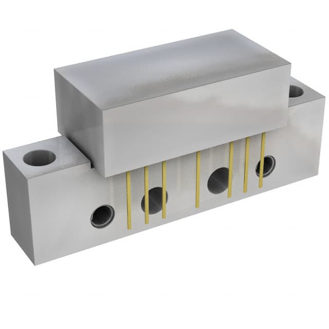
SOT115J package: rectangular single-ended aluminum flange with 7 gold-plated in-line leads, 2 vertical 6-32 UNC mounting holes, and thermal interface optimized for heatsink attachment.
| Pin/Terminal | Circuit Role | Design Meaning |
|---|---|---|
| 1 | RF input | 50 Ω matched input port; requires no external DC blocking for AC-coupled CATV signal injection |
| 2, 3 | Common ground | Dedicated low-inductance RF ground path for input stage stability and harmonic suppression |
| 5 | +VB supply | 24 V DC power input; decoupling capacitor must be placed within 5 mm for HFET bias stability |
| 7, 8 | Common ground | Output-stage ground return; isolated from input grounds to prevent feedback coupling |
| 9 | RF output | 75 Ω matched output; delivers flat 44 dBmV level across 40–1003 MHz with ≤0.9 dB ripple |
Key Features
| Feature | Design Value |
|---|---|
| Push-pull GaAs HFET topology | Eliminates need for external even-order cancellation networks, reducing BOM count and layout area in node designs |
| Integrated ring-wave surge protection | Withstands IEC 61000-4-5 Level 3 surges without external TVS, enabling direct drop-in replacement in legacy trunk amps |
| Thermally optimized aluminum flange | Enables 100 °C mounting base temperature operation with standard heatsinking-no forced air required |
| Unconditional stability | Guarantees oscillation-free operation across full 40–1003 MHz band without external stabilization components |
| RoHS-compliant construction | Meets Directive 2002/95/EC with lead-free finish and halogen-free molding compound for global cable infrastructure compliance |
Applications
| CATV Trunk Amplifier Stage | HFC Node Output Stage |
|---|---|
Use Scenario: Amplification of downstream signals in active trunk lines spanning >1 km between headend and optical nodes. IC Role / Device Role / Timing Role: Primary RF gain block delivering flat 21 dB gain across 40–1003 MHz with minimal CTB degradation under full channel load. Use Value: Enables 79 NTSC + 75 digital channel transmission at 44 dBmV with −62 dBc CTB, meeting SCTE-47 linearity requirements without post-compensation. |
Use Scenario: Final-stage amplification in fiber-deep HFC nodes feeding coaxial distribution to 500+ homes. IC Role / Device Role / Timing Role: High-reliability output driver with integrated surge protection for outdoor-rated node enclosures exposed to lightning-induced transients. Use Value: Eliminates need for discrete ring-wave protectors, reducing bill-of-materials and improving MTBF in field-deployed nodes. |
| CATV Optical Receiver Output | DOCSIS 3.1 Upstream Booster |
Use Scenario: Post-demodulation amplification in analog/digital optical receivers converting fiber input to 75 Ω coaxial output. IC Role / Device Role / Timing Role: Low-noise, high-return-loss buffer ensuring minimal signal degradation before splitting to multiple distribution legs. Use Value: Input return loss ≥19 dB up to 550 MHz prevents standing waves that distort QAM constellations in multi-leg splitters. |
Use Scenario: Boosting upstream return-path signals (5–85 MHz) in DOCSIS 3.1 nodes where SNR margin is critical for 256-QAM upstream modulation. IC Role / Device Role / Timing Role: Low-noise figure (3.6 dB typ.) amplifier preserving upstream carrier-to-noise ratio in noisy plant environments. Use Value: Maintains >63 dBc carrier-to-composite noise at 44 dBmV output, directly supporting upstream spectral efficiency targets. |
Equivalent & Alternatives
The following parts are listed as comparable options for similar RF amplifier applications.
| Alternative Part | Technical Difference | Application Difference | Selection Advice |
|---|---|---|---|
| CGY1042,112 | Same SOT115J package and pinout; 22.5 dB max gain at 1003 MHz but higher 290 mA current draw | Optimized for lower-distortion 98 PAL channel operation (−68 dBc CTB), not NTSC/digital mix | Select when PAL-based regional deployments require tighter CTB specs and thermal budget allows higher Itot |
| CGY1040,112 | Same footprint and bias; 19.5 dB typ. gain at 1003 MHz and −58 dBc CTB - lower linearity tier | Targeted for cost-sensitive tap amplifiers or short-span distribution where full 79+75 channel loading is not required | Choose for non-critical spans where 4 dB lower gain and 4 dB worse CTB are acceptable for BOM reduction |
Compared with CGY1041,112, CGY1042,112 trades higher current for superior PAL-channel CTB, while CGY1040,112 reduces gain and linearity to cut cost-making CGY1041,112 the balanced choice for global NTSC/digital hybrid CATV deployments requiring 21 dB gain and −62 dBc CTB at 24 V.
Availability
CGY1041,112 is available at Aetrix Electronics and suitable for CATV trunk amplifiers, HFC node output stages, optical receiver outputs, and DOCSIS 3.1 upstream boosters requiring stable component supply with full RoHS compliance and surge-hardened construction.
Supply support for CGY1041,112 includes scheduled delivery planning, volume procurement assistance, BOM continuity management, traceable sourcing, and lifecycle availability coordination for OEM customers, industrial embedded developers, connected-device designers, and electronics production programs.
Manufacturer
NXP Semiconductors is a global semiconductor leader specializing in secure connectivity solutions for automotive, industrial, and communications infrastructure markets, with core expertise in RF power and analog front-end technologies.
The CGY1041,112 belongs to NXP's CATV RF amplifier product line, engineered specifically for broadband cable infrastructure requiring high linearity, thermal resilience, and integrated surge protection in outdoor-deployed active components.
FAQ
What is the maximum operating temperature for the CGY1041,112 mounting base?
The CGY1041,112 supports a mounting base temperature (Tmb) up to +100 °C per its limiting values table. This rating is validated under continuous 24 V DC operation with proper heatsinking and enables deployment in sealed outdoor enclosures without active cooling. Derating is not required until Tmb exceeds 100 °C, and the device remains unconditionally stable across this full range.
Does the CGY1041,112 require external DC blocking capacitors on input or output?
No, the CGY1041,112 does not require external DC blocking capacitors on input (Pin 1) or output (Pin 9). Its internal biasing network is designed for direct AC-coupled connection to 75 Ω CATV signal paths. The datasheet specifies ZS = ZL = 75 Ω operation with no mention of DC path constraints, confirming true AC-coupled RF port functionality.
What is the flatness specification for the CGY1041,112 across its full bandwidth?
The CGY1041,112 exhibits ≤0.9 dB flatness (FL) across 45–1003 MHz, defined as maximum deviation from a straight-line fit. This tight ripple ensures uniform channel loading in 79 NTSC + 75 digital channel systems, preventing tilt-induced differential gain errors in analog video and constellation rotation in digital QAM carriers.
How does the integrated ring-wave surge protection in the CGY1041,112 compare to external TVS diodes?
The CGY1041,112 integrates ring-wave surge protection compliant with IEC 61000-4-5 Level 3, eliminating the need for discrete TVS devices typically rated at 10/700 µs waveform. Unlike external TVS solutions that add capacitance and insertion loss, the monolithic protection maintains RF performance integrity while reducing PCB area and assembly cost in trunk amplifier designs.
Is the CGY1041,112 pin-compatible with other members of the CGY10xx family?
Yes, the CGY1041,112 shares identical SOT115J pinout, footprint, and mounting hole pattern with CGY1040,112 and CGY1042,112. All three variants use Pins 1 (input), 2–3 and 7–8 (grounds), 5 (+VB), and 9 (output) with identical mechanical dimensions-enabling drop-in substitution in existing layouts when adjusting gain or linearity targets.
CGY1041,112 Specifications
- Product attributes
- Attribute value
- Manufacturer:
- NXP Semiconductors
- Package/Case:
- SOT-115J
- Series:
- -
- Packaging:
- Bulk
- Product Status:
- Obsolete
- Applications:
- CATV
- Output Type:
- -
- Number of Circuits:
- 1
- -3db Bandwidth:
- -
- Slew Rate:
- -
- Current - Supply:
- 265 mA
- Current - Output / Channel:
- -
- Voltage - Supply, Single/Dual (±):
- -
- Mounting Type:
- Chassis Mount
- Grade:
- -
- Qualification:
- -
- Supplier Device Package:
- SOT115J
CGY1041,112 FAQ
1.How can I place an order for CGY1041,112 through Aetrix?
Please submit a Request for Quotation (RFQ) for CGY1041,112 on Aetrix. Our sales agent will provide a competitive quotation and guide you through the order confirmation once you accept the terms.
2.Are the price and stock information for CGY1041,112 reliable?
The price and inventory of CGY1041,112 are updated periodically and may fluctuate due to market conditions. Stock and pricing data are typically refreshed every 24 hours. Quotation validity for CGY1041,112 is usually 5 days.
3.What payment methods are accepted for CGY1041,112?
We accept Wire Transfer, PayPal, Credit Card, Western Union, MoneyGram, and Escrow for CGY1041,112 transactions.
Note: Certain payment methods may incur a processing fee.
4.How is shipping managed for CGY1041,112?
CGY1041,112 orders can be shipped via leading logistics carriers, including DHL, UPS, FedEx, TNT, or Registered Mail.
Once your CGY1041,112 order is processed, you will receive an email with the shipment details and tracking number.
Note: Tracking information may take up to 24 hours to appear. Express delivery typically takes 3–5 business days.
5.How can I obtain technical support or documentation for CGY1041,112?
For technical support, including CGY1041,112 datasheets, pinout diagrams, or application guidance, please contact our engineering support team. They can provide detailed documentation and assistance for your CGY1041,112 requirements.
6.How does Aetrix verify that CGY1041,112 is sourced from the original manufacturer or authorized distributors?
All CGY1041,112 products on Aetrix are procured from qualified distributors and authorized channels. Our dedicated quality assurance team conducts strict verification, including traceability checks and, if necessary, third-party testing. This ensures that CGY1041,112 meets industry standards.
7.What is the process for return or replacement of CGY1041,112?
All CGY1041,112 units undergo pre-shipment inspection (PSI). If there is an issue with CGY1041,112, returns or replacements are accepted under the following conditions:
1.Quantity discrepancies, incorrect items, or visible external defects (such as breakage or corrosion), acknowledged by Aetrix.
2.The issue is reported within 90 days of delivery.
3.The CGY1041,112 part is unused and in its original packaging.
Return procedure for CGY1041,112:
1.Submit a request within 90 days.
2.Obtain a Return Material Authorization (RMA) from Aetrix.
CGY1041,112 Tags

-
LT6552CS8#PBF
Analog Devices Inc.
-
LT6205IS5#TRPBF
Analog Devices Inc.
-
LT6206IMS8#TRPBF
Analog Devices Inc.
-
LT6552CDD#PBF
Analog Devices Inc.
-
LT6552IS8#PBF
Analog Devices Inc.
-
LT1252CS8#PBF
Analog Devices Inc.
-
AD818ARZ-REEL7
Analog Devices Inc.

-
MAX4310EUA+
Analog Devices Inc./Maxim Integrated
-
AD829ARZ
Analog Devices Inc.
-
AD810ARZ
Analog Devices Inc.

-
MAX4310ESA+
Analog Devices Inc./Maxim Integrated
-
MAX4313ESA+
Analog Devices Inc./Maxim Integrated
Tech Hub

A practical engineering guide to 3.3V and 5V logic compatibility, input thresholds, resistor dividers, translator ICs, MOSFET level shifting, I2C pull-ups, timing limits and power-sequencing risks.

The 74HC595 uses push-pull logic outputs, while the TPIC6B595 uses 50 V open-drain DMOS sinks for higher-power loads. This guide compares timing, current limits, 3.3 V interfacing, load wiring, thermal…

The 74HC595 converts serial data into eight stable parallel outputs. This guide covers pin functions, shift and storage timing, OE and MR behavior, drive-current limits, cascading, voltage compatibilit…

A technical comparison of level-sensitive latches and edge-triggered flip-flops, covering timing windows, setup and hold limits, master–slave operation, time borrowing, race-through, HDL inference and…

A D latch stores one bit while Enable controls when data can pass. This reference covers gate-level operation, truth tables, transparency, setup and hold timing, LE versus OE, common ICs and practical …

An SR latch stores one bit through cross-coupled feedback. This engineering reference covers NOR and NAND implementations, truth tables, forbidden-state recovery, gated operation, switch debouncing, fa…

Latch circuits retain one bit through feedback. This technical reference covers SR and D latches, truth tables, transparency, timing limits, latch-versus-flip-flop behavior, applications and common log…

An engineering guide to LED driver operation, constant-current and constant-voltage outputs, linear and switching topologies, dimming, IC selection, calculations, replacement compatibility, and fault c…

Operational amplifier guide covering op amp basics, feedback, ideal vs real op amps, common configurations, buffer circuits, offset, bias current, gain-bandwidth, slew rate, rail-to-rail limits and sel…

Jumper cables guide covering safe connection order, red and black clamp placement, final ground connection, cable gauge, length, clamp quality, copper vs CCA cables, jump starter comparison and battery…


