
 My Inquiry
 My Account


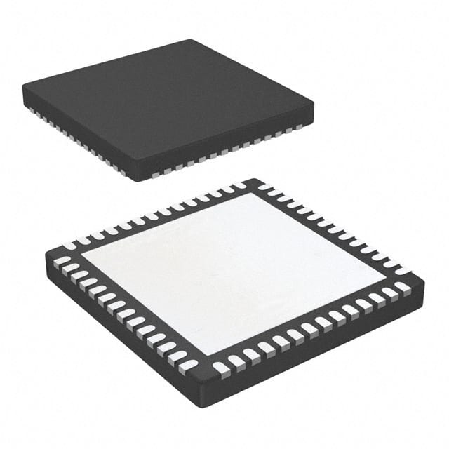
Infineon Technologies CHL8318-20-04CR
- Part No.:
- CHL8318-20-04CR
- Manufacturer:
- Infineon Technologies
- Category:
- DC DC Switching Controllers
- Package:
- 56-VFQFN Exposed Pad
- Datasheet:
-
 CHL8318-20-04CR.pdf
- Description:
- IC REG BUCK 56VQFN
- Quantity:
- Payment:

- Shipping:

Inventory:2,594
Please send an inquiry. Send us your inquiry, and we will respond immediately.
Product details
Overview
CHL8318-20-04CR from CHiL Semiconductor is an 8-phase digital synchronous buck controller compliant with Intel VR11.1/VR11.0 specifications, designed for CPU core voltage regulation in high-performance desktop and server platforms. It supports programmable 1–8-phase operation, 200 kHz–1 MHz per-phase switching frequency (±2% accuracy), SMBus-based gamer-mode VID control up to 2.3 V, and adaptive transient response for reduced bulk capacitance.
For engineers reviewing the CHL8318-20-04CR datasheet, CHL8318-20-04CR pinout, CHL8318-20-04CR application, or CHL8318-20-04CR equivalent, key selection considerations include VR11.x compliance, digital phase shedding (1–4-phase PSI), thermal phase balancing, sensorless input current monitoring (IMON), and NVM-configurable over-clocking features including Gamer OC/OVP and VID override.
Technical Context
The CHL8318-20-04CR implements a non-linear digital PWM architecture with adaptive transient control that dynamically adjusts duty cycle and phase count based on load step magnitude and slew rate. Its digital processor integrates eight independent PWM generators, a 10-bit ADC for voltage/current sensing, and three NTC temperature sensor interfaces (TSEN1–TSEN3) for VR_HOT and OTP fault reporting.
It uses a 3-pin SMBus interface (SCL/SDA/SALERT#) for real-time configuration and telemetry-including input current, power, OVP/UVP/OCP/OTP status-and supports tri-state gate drivers (e.g., CHL8510) with variable gate drive (VAR_GATE) for optimized MOSFET switching loss across load conditions.
Key Specifications
| Parameter | Value and Actual Design Meaning |
|---|---|
| Phases | Programmable 1–8 phases; enables dynamic phase add/drop for >90% efficiency across full load range. |
| Switching Frequency | 200 kHz–1 MHz per phase, ±2% accuracy; allows optimization of inductor size vs. efficiency trade-off. |
| Gamer VID Range | Up to 2.3 V with 6.25 mV resolution; supports overclocking without external DAC or resistor networks. |
| PSI Support | Configurable 1–4-phase PSI mode; reduces driver and inductor losses during light-load operation. |
| Temperature Sensing | Three NTC inputs (TSEN1–TSEN3); enables per-phase thermal monitoring and digital thermal phase balancing. |
| NVM Storage | 9 bytes on-chip non-volatile memory; stores configuration (e.g., load-line, OCP thresholds, gamer settings) for "set-and-forget" deployment. |
| Supply Voltage | +3.3 V nominal; operates from 0°C to +85°C ambient; eliminates need for auxiliary LDOs in VRD design. |
Pinout & Package
CHL8318-20-04CR is housed in an 8 mm × 8 mm, 56-pin QFN package with exposed thermal pad (MSL Level 1, RoHS compliant). Pin functions are validated per CHiL Semiconductor PB0006 Rev. 1.00.
| Pin/Terminal | Circuit Role | Design Meaning |
|---|---|---|
| PWM1–PWM8 | Phase PWM outputs | Eight independent gate-drive signals supporting interleaved multi-phase buck topology with 180° phase shift capability. |
| ISEN1–ISEN8 | Current sense inputs | Differential inputs for DCR or shunt-based per-phase current sensing; enable precise current balance and OCP protection. |
| IRTN1–IRTN8 | Current sense return | Individual low-impedance returns for each ISEN pair; minimize noise coupling and improve current measurement accuracy. |
| VID0–VID7 | VRD VID bus inputs | 8-bit parallel interface for CPU VID code reception; supports VR11.x dynamic voltage identification protocol. |
| SCL / SDA / SALERT# | SMBus interface | 3-wire system management bus for configuration, telemetry (IMON, temperature, faults), and gamer-mode activation. |
| TSEN1–TSEN3 | NTC temperature sensor inputs | Analog inputs for external NTC thermistors; used for VR_HOT assertion and digital thermal phase balancing algorithm. |
Key Features
| Feature | Design Value |
|---|---|
| Adaptive Transient Algorithm | Non-linear digital PWM response reduces required output bulk capacitance by up to 40% versus fixed-frequency controllers. |
| Variable Gate Drive (VAR_GATE) | Adjusts high-side/low-side gate drive strength dynamically to minimize switching loss at light and heavy loads. |
| Digital Thermal Phase Balancing | Proportional current redistribution between phases based on real-time temperature readings from TSEN1–TSEN3. |
| Gamer Mode via SMBus | Enables extended VID (2.3 V), digital load-line adjust, Gamer OC/OVP, and GAMER_OFF pin control without hardware modification. |
| Sensorless Input Current Monitoring | Derives input current (IMON) from PWM duty cycle and VINSEN without shunt resistor, reducing BOM cost and board space. |
Applications
| Intel VR11.x CPU VRD | High-Performance Desktop Platform |
|---|---|
Use Scenario: Core voltage regulation for Intel Core i7/i9 processors requiring VR11.1-compliant dynamic VID scaling and fast transient response. IC Role / Device Role / Timing Role: Primary digital multi-phase buck controller managing up to 8 power stages, PSI signaling, and IMON telemetry. Use Value: Enables <1% voltage deviation under 50 A/µs load steps while maintaining VR11.1 specification compliance and reducing bulk capacitor count by 30%. | Use Scenario: Overclocking-capable motherboard VRM delivering stable 1.4–2.3 V core voltage with real-time SMBus tuning. IC Role / Device Role / Timing Role: Configurable digital controller with Gamer Mode activation, VID override, and digital load-line adjustment. Use Value: Supports user-adjustable voltage/frequency curves via BIOS or software tools without hardware rework or external components. |
| Server CPU Power Delivery | Coupled-Inductor VRD Design |
Use Scenario: Dual-socket Xeon platform requiring thermal-aware phase management and fault telemetry across multiple VRDs. IC Role / Device Role / Timing Role: Multi-controller SMBus network node providing OVP/UVP/OCP/OTP status, temperature, and input power data to BMC. Use Value: Delivers traceable, time-stamped fault logs and enables predictive thermal derating via digital phase shedding. | Use Scenario: Space-constrained 1U server VRD using coupled inductors to reduce component height and improve transient response. IC Role / Device Role / Timing Role: Controller configured for 2-phase PSI and 180° out-of-phase phase add/drop to maximize inductor coupling benefit. Use Value: Achieves 25% smaller solution footprint and 35% faster load-step recovery vs. discrete inductor implementation. |
Equivalent & Alternatives
The following parts are listed as comparable options for similar multi-phase digital buck controller applications.
| Alternative Part | Technical Difference | Application Difference | Selection Advice |
|---|---|---|---|
| ISL6367IRZ | 7-phase, VR12.0/IMVP7 compliant; lacks Gamer Mode and extended 2.3 V VID; uses analog current sensing. | Targeted at post-VR11 platforms with tighter voltage tolerance (±5 mV) but no overclocking focus. | Select when VR12.0 compliance and lower voltage ripple are prioritized over gamer configurability. |
| MP2940AGQSE | 8-phase, VR11.1-compliant; includes SMBus but no NVM storage or digital thermal balancing; limited to 1.55 V max VID. | Cost-optimized VRD for mainstream desktops; omits advanced overclocking features and phase-level temperature feedback. | Select when basic VR11.1 functionality and SMBus telemetry suffice without customization or thermal intelligence. |
Compared with ISL6367IRZ and MP2940AGQSE, the CHL8318-20-04CR uniquely combines VR11.1 compliance, on-chip NVM for persistent gamer settings, digital thermal phase balancing, and 2.3 V extended VID-making it the only option for high-end overclocking VRDs requiring field-updatable, thermally aware multi-phase control.
Availability
CHL8318-20-04CR is available at Aetrix Electronics and suitable for Intel VR11.x CPU VRD designs, high-performance desktop motherboards, and server power delivery systems requiring stable component supply, long-term lifecycle support, and consistent electrical performance across production batches.
Supply support for CHL8318-20-04CR includes scheduled delivery planning, volume procurement assistance, BOM continuity management, traceable sourcing, and lifecycle availability coordination for OEM customers, industrial embedded developers, connected-device designers, and electronics production programs.
Manufacturer
CHiL Semiconductor Corp., headquartered in Tewksbury, MA, specializes in digitally controlled power management ICs for high-efficiency computing and server applications.
The CHL8318 product line was developed specifically for Intel VR11.x-compliant CPU voltage regulation, emphasizing configurability, thermal intelligence, and overclocking readiness in compact multi-phase VRD implementations.
FAQ
What is the maximum supported VID voltage and resolution in Gamer Mode?
The CHL8318-20-04CR supports up to 2.3 V in Gamer Mode with 6.25 mV resolution, enabled via SMBus command without external components. This extends beyond standard VR11.x VID limits (1.55 V) and is stored in on-chip NVM for persistent configuration across power cycles.
Does CHL8318-20-04CR require external current-sense resistors?
No-it supports both DCR-based and shunt-based current sensing. The ISEN1–ISEN8 inputs accept differential signals from either method, and its sensorless input current monitor (IMON) derives total input current from PWM duty cycle and VINSEN, eliminating the need for a dedicated input shunt in many designs.
How does digital thermal phase balancing function in practice?
Digital thermal phase balancing uses real-time temperature readings from TSEN1–TSEN3 to proportionally redistribute current among active phases-e.g., reducing current in hotter phases and increasing it in cooler ones-without interrupting regulation. This maintains output stability while extending MOSFET lifetime and enabling higher sustained power density.
Can CHL8318-20-04CR operate with fewer than 8 phases in a production design?
Yes-it is fully configurable for 1–8 phases via SMBus or NVM. Common configurations include 4-phase for mainstream desktops and 6- or 8-phase for high-end gaming/server CPUs. Phase count is set at startup and can be dynamically adjusted during operation based on load and thermal conditions.
CHL8318-20-04CR Specifications
- Product attributes
- Attribute value
- Manufacturer:
- Infineon Technologies
- Series:
- -
- Package/Case:
- 56-VFQFN Exposed Pad
- Packaging:
- Tape & Reel (TR)
- Product Status:
- Obsolete
- Output Type:
- PWM
- Function:
- Step-Down
- Output Configuration:
- Positive
- Topology:
- Buck
- Number of Outputs:
- 1
- Output Phases:
- 8
- Voltage - Supply (Vcc/Vdd):
- 3.3V
- Frequency - Switching:
- 200kHz ~ 1MHz
- Duty Cycle (Max):
- -
- Synchronous Rectifier:
- No
- Clock Sync:
- No
- Serial Interfaces:
- SMBus
- Control Features:
- Enable
- Operating Temperature:
- 0°C ~ 85°C (TA)
- Grade:
- -
- Qualification:
- -
- Mounting Type:
- Surface Mount
- Supplier Device Package:
- PG-VQFN-56-901
CHL8318-20-04CR FAQ
1.How can I place an order for CHL8318-20-04CR through Aetrix?
Please submit a Request for Quotation (RFQ) for CHL8318-20-04CR on Aetrix. Our sales agent will provide a competitive quotation and guide you through the order confirmation once you accept the terms.
2.Are the price and stock information for CHL8318-20-04CR reliable?
The price and inventory of CHL8318-20-04CR are updated periodically and may fluctuate due to market conditions. Stock and pricing data are typically refreshed every 24 hours. Quotation validity for CHL8318-20-04CR is usually 5 days.
3.What payment methods are accepted for CHL8318-20-04CR?
We accept Wire Transfer, PayPal, Credit Card, Western Union, MoneyGram, and Escrow for CHL8318-20-04CR transactions.
Note: Certain payment methods may incur a processing fee.
4.How is shipping managed for CHL8318-20-04CR?
CHL8318-20-04CR orders can be shipped via leading logistics carriers, including DHL, UPS, FedEx, TNT, or Registered Mail.
Once your CHL8318-20-04CR order is processed, you will receive an email with the shipment details and tracking number.
Note: Tracking information may take up to 24 hours to appear. Express delivery typically takes 3–5 business days.
5.How can I obtain technical support or documentation for CHL8318-20-04CR?
For technical support, including CHL8318-20-04CR datasheets, pinout diagrams, or application guidance, please contact our engineering support team. They can provide detailed documentation and assistance for your CHL8318-20-04CR requirements.
6.How does Aetrix verify that CHL8318-20-04CR is sourced from the original manufacturer or authorized distributors?
All CHL8318-20-04CR products on Aetrix are procured from qualified distributors and authorized channels. Our dedicated quality assurance team conducts strict verification, including traceability checks and, if necessary, third-party testing. This ensures that CHL8318-20-04CR meets industry standards.
7.What is the process for return or replacement of CHL8318-20-04CR?
All CHL8318-20-04CR units undergo pre-shipment inspection (PSI). If there is an issue with CHL8318-20-04CR, returns or replacements are accepted under the following conditions:
1.Quantity discrepancies, incorrect items, or visible external defects (such as breakage or corrosion), acknowledged by Aetrix.
2.The issue is reported within 90 days of delivery.
3.The CHL8318-20-04CR part is unused and in its original packaging.
Return procedure for CHL8318-20-04CR:
1.Submit a request within 90 days.
2.Obtain a Return Material Authorization (RMA) from Aetrix.
CHL8318-20-04CR Tags

-
UCC28C45DR
Texas Instruments
-
UCC28C40DR
Texas Instruments
-
UCC28C43DR
Texas Instruments

-
ZXSC410E6TA
Diodes Incorporated

-
LM3524DMX/NOPB
Texas Instruments

-
LM3489MMX/NOPB
Texas Instruments
-
MIC2102YML-TR
Microchip Technology

-
LM5148RGYR
Texas Instruments
-
TL598CDR
Texas Instruments

-
LM5155DSSR
Texas Instruments

-
LM25085MYX/NOPB
Texas Instruments
-
UCC2813DTR-0
Texas Instruments
Tech Hub

An engineering guide to LED driver operation, constant-current and constant-voltage outputs, linear and switching topologies, dimming, IC selection, calculations, replacement compatibility, and fault c…

Operational amplifier guide covering op amp basics, feedback, ideal vs real op amps, common configurations, buffer circuits, offset, bias current, gain-bandwidth, slew rate, rail-to-rail limits and sel…

Jumper cables guide covering safe connection order, red and black clamp placement, final ground connection, cable gauge, length, clamp quality, copper vs CCA cables, jump starter comparison and battery…

LDO regulator guide covering low dropout voltage, power dissipation, thermal design, PSRR, output noise, capacitor stability, adjustable LDO circuits, LDO vs buck converter and datasheet selection chec…

Conditional Access Module guide covering CAM meaning, CI/CI+ interface, smart card authorization, DVB security workflow, TV and set-top box compatibility, internal electronics, ESD protection, connecto…

Guide to electronic component obsolescence covering EOL risk, PCN/PDN notices, last-time buy planning, replacement options, form-fit-function validation, counterfeit risk and BOM lifecycle management.

18650 battery guide covering lithium-ion cell basics, 3.6V/3.7V voltage, 4.2V charging, mAh and Wh capacity, protected cells, chargers, BMS, series-parallel packs, holders, welding and sourcing checks.…

Hall effect sensor guide covering working principle, linear and digital sensors, Arduino circuits, current sensing, speed detection, automotive applications, A3144 examples, signal filtering and datash…

Product Change Notification guide for electronic components, covering PCN meaning, PCN vs PDN/EOL, common change types, risk levels, form-fit-function review, engineering validation, BOM control, LTB/L…

A practical guide to blend door actuators, covering HVAC function, symptoms, location, AC and heater issues, reset and calibration, replacement cost, electrical diagnosis, compatibility checks, and rep…


