
 My Inquiry
 My Account


onsemi CMPWR330SF
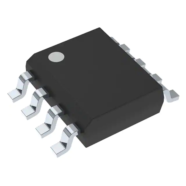
- Part No.:
- CMPWR330SF
- Manufacturer:
- onsemi
- Package:
- 8-SOIC (0.154", 3.90mm Width)
- Datasheet:
-
 CMPWR330SF.pdf
- Description:
- IC REG LINEAR 3.3V 400MA 8SOIC
- Quantity:
- Payment:

- Shipping:

Inventory:4,742
Please send an inquiry. Send us your inquiry, and we will respond immediately.
Product details
Overview
CMPWR330SF from onsemi is a dual-input 3.3 V SmartOR regulator with integrated VAUX switch, delivering up to 400 mA continuously. It selects power from VCC (5 V), VSBY (5 V), or VAUX (3.3 V) in strict priority order and provides low-impedance VAUX-to-VOUT pass-through (0.25 Ω typ.) when only VAUX is active. Used in PCI adapter cards with Wake-on-LAN for seamless standby-to-active transitions.
For engineers reviewing the CMPWR330SF datasheet, pinout, applications, or equivalent options, key selection criteria include input supply prioritization logic, 0.25 Ω VAUX switch RDS(ON), foldback current limiting, thermal shutdown at 160°C, and compatibility with 8-pin Power SOIC layout constraints.
Technical Context
The CMPWR330SF implements automatic input source selection using comparator-based control with 4.4 V VCC select threshold and 4.2 V deselect threshold, yielding 0.2 V hysteresis to prevent chatter. Its internal regulator delivers regulated 3.3 V ±5% over 0–400 mA load, while the VAUX path operates as a low-RDS(ON) MOSFET switch-not a linear regulator-enabling direct 3.3 V pass-through.
Power sequencing is fully autonomous: VCC takes precedence; if VCC drops below 4.2 V and VSBY is present, VSBY powers the regulator; if both VCC and VSBY are absent, VAUX connects directly to VOUT. All transitions maintain uninterrupted VOUT via internal charge management and 10 µF output capacitance requirement.
Key Specifications
| Parameter | Value and Actual Design Meaning |
|---|---|
| Output Voltage | 3.30 V ±5% (3.135–3.465 V); stable regulation across full 0–400 mA load range |
| VAUX Switch RDS(ON) | 0.25 Ω typical; enables <1 mV drop at 400 mA, preserving VAUX rail integrity |
| VCC Select Threshold | 4.40–4.60 V; ensures clean handover from VSBY/VAUX to main 5 V rail |
| Current Limit | 500 mA min; foldback protection reduces output current during overload to limit power dissipation |
| Thermal Shutdown | 160°C junction temperature; hysteresis of 20°C prevents oscillation near trip point |
| Operating Temp Range | 0°C to +70°C ambient; supports industrial-grade embedded systems without derating |
| Package Thermal Resistance | 50°C/W (with 2 in² copper heat spread); enables 0.7 W dissipation at 70°C ambient |
Pinout & Package
CMPPWR330SF is housed in an 8-pin Power SOIC package (Case 751BD), thermally enhanced with pins 5–8 tied to the exposed leadframe for GND and heat dissipation. The package complies with JEDEC MS-012 and features RoHS-compliant lead-free finish.
| Pin/Terminal | Circuit Role | Design Meaning |
|---|---|---|
| 1 - VSBY | Standby input supply (5 V) | Second-priority input; powers regulator when VCC < 4.2 V; requires ≤0.3 Ω source impedance for stable switching |
| 2 - VCC | Main input supply (5 V) | First-priority input; enables regulator above 4.4 V; hysteresis prevents bounce during brownout |
| 3 - VOUT | Regulated 3.3 V output | Delivers up to 400 mA; requires 10 µF ceramic capacitor for stability and transient suppression |
| 4 - VAUX | Auxiliary input (3.3 V) | Third-priority input; directly connected to VOUT via internal switch when VCC/VSBY absent |
| 5–8 - GND | Ground reference & thermal path | All four pins bonded to leadframe; mandatory connection to ≥2 in² copper pour for thermal performance |
Key Features
| Feature | Design Value |
|---|---|
| Triple-input priority arbitration | Hardware-enforced VCC → VSBY → VAUX selection with no external logic or firmware required |
| Integrated VAUX pass switch | 0.25 Ω RDS(ON) eliminates need for discrete MOSFET and gate driver in auxiliary path |
| Foldback current limiting | Reduces output current progressively under short-circuit, limiting peak power to <0.3 W |
| Thermal overload protection | Shuts down at 160°C junction; restarts automatically after 20°C cooldown, preventing latch-up |
| Low quiescent current | 0.8–1.5 mA (VCC/VSBY active), 0.2–0.3 mA (VAUX-only mode); minimizes standby power loss |
Applications
| PCI Adapter Cards with Wake-on-LAN | Network Interface Cards (NICs) |
|---|---|
Use Scenario: Desktop add-in card remains powered in S3/S4 sleep states while monitoring network traffic for magic packet wake events. IC Role / Device Role / Timing Role: SmartOR regulator maintains stable 3.3 V VCCIO for PHY and MAC logic using VAUX during deep sleep, then seamlessly switches to VCC upon wake. Use Value: Eliminates need for separate VAUX LDO and OR-ing diodes; 0.25 Ω VAUX switch ensures <1 mV droop at 400 mA, preserving signal integrity. |
Use Scenario: Embedded NIC in server blade draws power from multiple rails: main 5 V (VCC), standby 5 V (VSBY), and auxiliary 3.3 V (VAUX) for management controller. IC Role / Device Role / Timing Role: Provides fault-tolerant 3.3 V supply with automatic fallback between redundant inputs without software intervention. Use Value: Enables hot-swap capability and graceful degradation: loss of VCC triggers immediate VSBY takeover; loss of both engages VAUX path within microseconds. |
| Multiple Power Systems | Systems with Standby Capabilities |
Use Scenario: Industrial gateway with isolated 5 V system rail, 5 V standby rail, and battery-backed 3.3 V real-time clock domain. IC Role / Device Role / Timing Role: Supplies 3.3 V to RTC, nonvolatile memory, and wake logic from highest-available input, ensuring continuous operation across power modes. Use Value: Built-in hysteresis (0.2 V) prevents oscillation during marginal VCC conditions; reverse leakage <100 nA preserves battery life in VAUX-only mode. |
Use Scenario: Set-top box enters low-power standby while retaining HDMI CEC and IR receiver functionality. IC Role / Device Role / Timing Role: Delivers regulated 3.3 V to always-on peripherals from VAUX during standby, then transitions to VCC/VSBY during full operation. Use Value: Integrated thermal shutdown (160°C) and foldback current limit protect against sustained overloads during unexpected wake events. |
Equivalent & Alternatives
The following parts are listed as comparable options for similar dual-input power management applications.
| Alternative Part | Technical Difference | Application Difference | Selection Advice |
|---|---|---|---|
| TPS2113AIDGQR | Single-channel 5-V ORing controller; no integrated regulator; requires external 3.3 V LDO | Supports only two inputs (no VAUX priority tier); lacks built-in 3.3 V regulation | Choose when system already has dedicated 3.3 V LDO and only needs input arbitration |
| RT9711CGQW | 3.3 V SmartOR with 600 mA rating; uses different priority logic (V1→V2 only); no VAUX pass-through mode | Designed for dual-rail 5 V systems; cannot accept 3.3 V auxiliary input as primary source | Choose when higher current (600 mA) is needed and VAUX is not part of power architecture |
Compared with TPS2113AIDGQR and RT9711CGQW, the CMPWR330SF uniquely integrates both 400 mA 3.3 V regulation and true three-tier priority (VCC→VSBY→VAUX) with low-RDS(ON) VAUX pass-through-enabling single-component solutions for systems requiring auxiliary 3.3 V sourcing without external regulators or switches.
Availability
CMPWR330SF is available at Aetrix Electronics and suitable for PCI adapter cards with Wake-on-LAN, network interface cards (NICs), and systems with standby capabilities requiring stable component supply across automotive-grade temperature ranges and long-lifecycle production programs.
Supply support for CMPWR330SF includes scheduled delivery planning, volume procurement assistance, BOM continuity management, traceable sourcing, and lifecycle availability coordination for OEM customers, industrial embedded developers, connected-device designers, and electronics production programs.
Manufacturer
onsemi (formerly ON Semiconductor) is a global semiconductor supplier focused on energy-efficient innovation for automotive, industrial, cloud, and intelligent edge applications.
The CMPWR330SF belongs to onsemi's SmartOR™ family of power-path controllers, designed specifically for seamless multi-rail power management in systems requiring reliable wake-from-standby operation without software intervention.
FAQ
What is the exact function of the VAUX pin on the CMPWR330SF?
The VAUX pin on the CMPWR330SF serves as the third-priority 3.3 V input source. When both VCC and VSBY are absent or below their respective thresholds, the CMPWR330SF enables an internal low-RDS(ON) switch (0.25 Ω typical) to connect VAUX directly to VOUT. This pass-through mode avoids regulation losses and preserves VAUX rail accuracy, making it ideal for battery-backed or auxiliary 3.3 V domains. The CMPWR330SF does not regulate VAUX-it routes it.
Does the CMPWR330SF require external components for stable operation?
Yes-the CMPWR330SF requires a 10 µF ceramic capacitor at VOUT for loop stability and transient suppression during input source transitions. Bypass capacitors (1–10 µF) are recommended at VCC and VSBY if traces exceed a few inches from the main input filter. No external compensation or feedback resistors are needed, as regulation and switching logic are fully integrated. The CMPWR330SF operates autonomously with these minimal external parts.
How does the CMPWR330SF handle simultaneous presence of VCC and VSBY?
The CMPWR330SF gives absolute priority to VCC over VSBY. If VCC exceeds 4.4 V, it powers the regulator regardless of VSBY status. VSBY only becomes active when VCC falls below 4.2 V. The 0.2 V hysteresis between select (4.4 V) and deselect (4.2 V) thresholds prevents oscillation during marginal VCC conditions. VSBY never powers the device while VCC is valid-even if VSBY voltage is higher-ensuring deterministic behavior. This logic is hardwired and requires no configuration.
What thermal design considerations apply to the CMPWR330SF?
The CMPWR330SF uses an 8-pin Power SOIC package with pins 5–8 internally connected to the leadframe as GND and thermal paths. To achieve the specified 50°C/W junction-to-ambient thermal resistance, at least 2 in² of copper area must be connected to these GND pins on a double-sided PCB. Without this, θJA rises to 70°C/W, limiting safe power dissipation. The CMPWR330SF includes thermal shutdown at 160°C with 20°C hysteresis, but proper board-level heatsinking is required for continuous 400 mA operation at 70°C ambient.
Can the CMPWR330SF be used in automotive applications?
The CMPWR330SF is specified for 0°C to +70°C ambient operation and is not qualified to AEC-Q100 standards. While its electrical characteristics (e.g., 6 V absolute max input, ±2 kV HBM ESD) provide margin beyond typical automotive requirements, onsemi does not certify or recommend the CMPWR330SF for automotive use. For automotive infotainment or body control modules requiring multi-rail power management, onsemi offers AEC-Q100-qualified alternatives such as the NCV8853. The CMPWR330SF targets industrial, computing, and networking applications.
CMPWR330SF Specifications
- Product attributes
- Attribute value
- Manufacturer:
- onsemi
- Series:
- SmartOR™
- Package/Case:
- 8-SOIC (0.154", 3.90mm Width)
- Packaging:
- Tape & Reel (TR)
- Product Status:
- Obsolete
- Output Configuration:
- Positive
- Output Type:
- Fixed
- Number of Regulators:
- 1
- Voltage - Input (Max):
- 5.25V
- Voltage - Output (Min/Fixed):
- 3.3V
- Voltage - Output (Max):
- -
- Voltage Dropout (Max):
- -
- Current - Output:
- 400mA
- Current - Quiescent (Iq):
- 1.5 mA
- Current - Supply (Max):
- -
- PSRR:
- -
- Control Features:
- -
- Protection Features:
- Over Current, Over Temperature
- Operating Temperature:
- 0°C ~ 70°C
- Grade:
- -
- Qualification:
- -
- Mounting Type:
- Surface Mount
- Supplier Device Package:
- 8-SOIC
CMPWR330SF FAQ
1.How can I place an order for CMPWR330SF through Aetrix?
Please submit a Request for Quotation (RFQ) for CMPWR330SF on Aetrix. Our sales agent will provide a competitive quotation and guide you through the order confirmation once you accept the terms.
2.Are the price and stock information for CMPWR330SF reliable?
The price and inventory of CMPWR330SF are updated periodically and may fluctuate due to market conditions. Stock and pricing data are typically refreshed every 24 hours. Quotation validity for CMPWR330SF is usually 5 days.
3.What payment methods are accepted for CMPWR330SF?
We accept Wire Transfer, PayPal, Credit Card, Western Union, MoneyGram, and Escrow for CMPWR330SF transactions.
Note: Certain payment methods may incur a processing fee.
4.How is shipping managed for CMPWR330SF?
CMPWR330SF orders can be shipped via leading logistics carriers, including DHL, UPS, FedEx, TNT, or Registered Mail.
Once your CMPWR330SF order is processed, you will receive an email with the shipment details and tracking number.
Note: Tracking information may take up to 24 hours to appear. Express delivery typically takes 3–5 business days.
5.How can I obtain technical support or documentation for CMPWR330SF?
For technical support, including CMPWR330SF datasheets, pinout diagrams, or application guidance, please contact our engineering support team. They can provide detailed documentation and assistance for your CMPWR330SF requirements.
6.How does Aetrix verify that CMPWR330SF is sourced from the original manufacturer or authorized distributors?
All CMPWR330SF products on Aetrix are procured from qualified distributors and authorized channels. Our dedicated quality assurance team conducts strict verification, including traceability checks and, if necessary, third-party testing. This ensures that CMPWR330SF meets industry standards.
7.What is the process for return or replacement of CMPWR330SF?
All CMPWR330SF units undergo pre-shipment inspection (PSI). If there is an issue with CMPWR330SF, returns or replacements are accepted under the following conditions:
1.Quantity discrepancies, incorrect items, or visible external defects (such as breakage or corrosion), acknowledged by Aetrix.
2.The issue is reported within 90 days of delivery.
3.The CMPWR330SF part is unused and in its original packaging.
Return procedure for CMPWR330SF:
1.Submit a request within 90 days.
2.Obtain a Return Material Authorization (RMA) from Aetrix.
CMPWR330SF Tags

-
MIC5504-1.8YM5-TR
Microchip Technology
-
MIC5504-3.3YM5-TR
Microchip Technology

-
MIC5365-3.0YC5-TR
Microchip Technology
-
MIC5365-1.8YC5-TR
Microchip Technology
-
MIC5365-2.5YC5-TR
Microchip Technology
-
MIC5365-3.3YC5-TR
Microchip Technology

-
MIC5365-3.3YD5-TR
Microchip Technology

-
MIC5317-3.3YM5-TR
Microchip Technology

-
TLV1117LV33DCYR
Texas Instruments

-
MIC5317-3.3YMT-TZ
Microchip Technology

-
MIC5528-3.3YMT-TR
Microchip Technology

-
TLV75801PDRVR
Texas Instruments
Tech Hub

Counterfeit components can hide behind convincing markings and passing basic function tests. This engineering reference covers source traceability, external inspection, X-ray, XRF, electrical testing, …

A practical engineering and sourcing framework covering lifecycle verification, lifetime-buy calculations, replacement qualification, supplier checks and counterfeit-risk controls.

TTL and CMOS logic families differ in thresholds, loading, output drive, power and timing. This engineering guide compares 74HC and 74HCT, calculates noise margins and checks 3.3 V/5 V compatibility.

A practical engineering guide to 3.3V and 5V logic compatibility, input thresholds, resistor dividers, translator ICs, MOSFET level shifting, I2C pull-ups, timing limits and power-sequencing risks.

The 74HC595 uses push-pull logic outputs, while the TPIC6B595 uses 50 V open-drain DMOS sinks for higher-power loads. This guide compares timing, current limits, 3.3 V interfacing, load wiring, thermal…

The 74HC595 converts serial data into eight stable parallel outputs. This guide covers pin functions, shift and storage timing, OE and MR behavior, drive-current limits, cascading, voltage compatibilit…

A technical comparison of level-sensitive latches and edge-triggered flip-flops, covering timing windows, setup and hold limits, master–slave operation, time borrowing, race-through, HDL inference and…

A D latch stores one bit while Enable controls when data can pass. This reference covers gate-level operation, truth tables, transparency, setup and hold timing, LE versus OE, common ICs and practical …

An SR latch stores one bit through cross-coupled feedback. This engineering reference covers NOR and NAND implementations, truth tables, forbidden-state recovery, gated operation, switch debouncing, fa…

Latch circuits retain one bit through feedback. This technical reference covers SR and D latches, truth tables, transparency, timing limits, latch-versus-flip-flop behavior, applications and common log…


