
 My Inquiry
 My Account


Renesas CP80C88-2Z
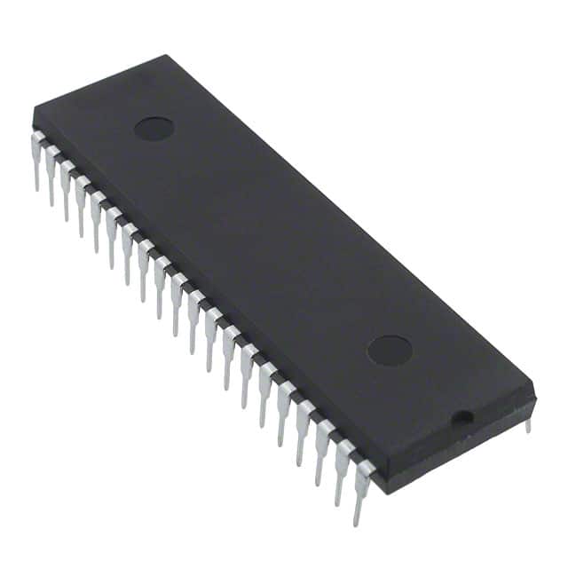
- Part No.:
- CP80C88-2Z
- Manufacturer:
- Renesas
- Category:
- Microprocessors
- Package:
- 40-DIP (0.600", 15.24mm)
- Datasheet:
-
 CP80C88-2Z.pdf
- Description:
- IC MPU 8MHZ 40DIP
- Quantity:
- Payment:

- Shipping:

Inventory:184
Please send an inquiry. Send us your inquiry, and we will respond immediately.
Product details
Overview
CP80C88-2Z from Intersil is a static CMOS 8-bit external data bus / 16-bit internal architecture microprocessor, operating up to 8 MHz with 1 MB direct memory addressing, 24 operand addressing modes, and full software compatibility with 8086/8088/80C86 for legacy x86 embedded control systems.
For engineers reviewing the CP80C88-2Z datasheet, CP80C88-2Z pinout, CP80C88-2Z application, or CP80C88-2Z equivalent, this page delivers verified electrical specs, minimum/maximum mode configuration details, bus-hold circuitry behavior, static operation support, and real-world use cases in industrial controllers and retro-computing platforms.
Technical Context
The CP80C88-2Z implements a two-unit architecture: Bus Interface Unit (BIU) with 4-byte instruction queue and Execution Unit (EU) with 16-bit ALU and register file. It supports both Minimum mode (single-processor) and Maximum mode (multiprocessor) via MN/MX pin, enabling flexible system scaling.
Its static CMOS design allows DC-to-8 MHz operation, zero-refresh memory access, and clock halt capability for debug or ultra-low-power states. Bus-hold circuitry on AD7–AD0 eliminates external pull-ups, while LOCK, RQ/GT, and QS0/QS1 signals enable co-processor coordination and instruction queue visibility.
Key Specifications
| Parameter | Value and Actual Design Meaning |
|---|---|
| Max Clock Frequency | 8 MHz - Enables higher throughput than 5 MHz CP80C88 variant in time-critical I/O cycles. |
| Data Bus Width | 8-bit multiplexed AD7–AD0 - Reduces PCB trace count vs. 16-bit bus; requires external latch (e.g., 82C82) on ALE. |
| Address Bus Width | 20-bit (A0–A19) - Supports full 1 MB linear memory space without banking or segmentation overhead. |
| Power Consumption | ICCOP ≤ 10 mA/MHz - Scales linearly with clock speed; enables predictable thermal budgeting in sealed enclosures. |
| Standby Current | ICCSB ≤ 500 µA - Allows battery-backed suspend mode in portable instrumentation or remote telemetry nodes. |
| Operating Temperature | 0°C to +70°C - Qualified for commercial-grade industrial control panels and laboratory equipment. |
| Package | 40-pin PDIP (Plastic Dual-In-Line), Pb-free RoHS-compliant - Compatible with through-hole prototyping and legacy wave-solder assembly. |
Pinout & Package
CP80C88-2Z uses a 40-lead PDIP package (drawing E40.6), with dual ground (Pins 1, 20) and VCC (Pin 40), 8-bit multiplexed address/data bus (AD7–AD0, Pins 9–16), and mode-selectable control signals including MN/MX (Pin 33), RD (Pin 32), WR (Pin 29), and ALE (Pin 25).
| Pin/Terminal | Circuit Role | Design Meaning |
|---|---|---|
| AD7–AD0 (Pins 9–16) | Multiplexed Address/Data Bus | Carries low-order address (T1) then data (T2–T4); requires external latch triggered by ALE pulse. |
| A8–A15 (Pins 2–8, 39) | Upper Address Bus | Provides stable high-order address bits throughout bus cycle; no latching needed. |
| A16/S3–A19/S6 (Pins 35–38) | Address/Status Multiplex | Delivers top 4 address bits in T1; outputs segment status (S3–S6) during T2–T4 in memory/I/O cycles. |
| MN/MX (Pin 33) | Mode Selection Input | High = Minimum mode (integrated control signals); Low = Maximum mode (external bus controller required). |
| RD (Pin 32), WR (Pin 29) | Read/Write Strobes | Active-low, timing-aligned signals controlling peripheral read/write timing in Minimum mode. |
| CLK (Pin 19) | Asymmetric Clock Input | 33% duty cycle (1/3 high, 2/3 low); enables optimized internal timing without external divider. |
| RESET (Pin 21) | Asynchronous Reset Input | Must be held high ≥4 clocks to initialize CS=FFFFH, IP=0000H and begin execution at FFFF0H. |
Key Features
| Feature | Design Value |
|---|---|
| Full software compatibility with 8086/8088/80C86 | Enables drop-in replacement in existing x86 BIOS, DOS, and real-mode firmware without recompilation. |
| Static CMOS architecture | Supports true DC operation and indefinite clock halt-critical for JTAG debug, power-gating, and battery backup. |
| Bus-hold circuitry on AD7–AD0 | Eliminates need for 8 external pull-up resistors, reducing BOM cost and board area in space-constrained designs. |
| Two operational modes (Minimum/Maximum) | Minimum mode simplifies single-CPU systems; Maximum mode enables multiprocessing via RQ/GT and LOCK protocols. |
| Instruction queue visibility (QS0/QS1) | Allows external logic to monitor BIU prefetch state-enabling cycle-accurate DMA arbitration and cache coherency. |
Applications
| Industrial PLC Controller | Retro-Computing Emulation Board |
|---|---|
Use Scenario: Standalone programmable logic controller executing ladder logic in factory automation cabinets with ambient temperatures up to +65°C. IC Role / Device Role / Timing Role: Primary CPU executing real-time I/O scan cycles, managing discrete input/output registers, and servicing interrupt-driven sensor events. Use Value: 8 MHz clock headroom ensures deterministic 10 ms scan intervals; static operation allows safe watchdog-triggered reset without memory corruption. |
Use Scenario: FPGA-based IBM PC XT clone reproducing original 8088 timing and bus protocol for authentic vintage software execution. IC Role / Device Role / Timing Role: Pin- and cycle-accurate CPU core interfacing with 74LS-series glue logic, DRAM refresh controller, and ISA-compatible peripherals. Use Value: Identical pinout and AC timing to NMOS 8088 enables faithful hardware replication; bus-hold eliminates need for legacy pull-ups on data lines. |
| Legacy Medical Instrumentation | Avionics Test Fixture Controller |
Use Scenario: Embedded controller in discontinued patient monitor handling serial ECG waveform acquisition and display update under IEC 60601 constraints. IC Role / Device Role / Timing Role: Real-time data aggregator routing analog front-end samples to SRAM buffer and driving segmented LCD via parallel interface. Use Value: 0°C to +70°C rating matches medical enclosure thermal profile; 1 MB addressing supports dual-buffered waveform storage without bank switching. |
Use Scenario: Self-contained test adapter verifying ARINC 429 transceiver functionality using discrete logic and minimal external components. IC Role / Device Role / Timing Role: Deterministic bus master coordinating timing-critical ARINC word transmission, parity generation, and response validation. Use Value: LOCK signal guarantees exclusive bus access during critical 32-bit ARINC word writes; static operation enables precise 100 µs inter-word gaps. |
Equivalent & Alternatives
The following parts are listed as comparable options for similar 8-bit x86 microprocessor applications.
| Alternative Part | Technical Difference | Application Difference | Selection Advice |
|---|---|---|---|
| CP80C86-2Z | 16-bit external data bus; identical 8 MHz rating and instruction set but higher pin count (40-pin same package, different pinout). | Requires wider PCB traces and different address latch (e.g., 82C83 instead of 82C82); supports faster memory access but increases layout complexity. | Select when system memory bandwidth > 2 MB/s is required and board layout accommodates full 16-bit bus. |
| Intel 8088-2 | NMOS process; higher ICCOP (15 mA/MHz), no bus-hold, no static operation, and narrower temperature range (0°C to +70°C only). | Lacks clock halt and true DC operation; requires external pull-ups and active cooling above 5 MHz; not RoHS-compliant. | Select only for strict NMOS 8088 footprint compliance where CMOS advantages are secondary to legacy sourcing. |
Compared with CP80C88-2Z, CP80C86-2Z delivers higher data throughput at the cost of layout complexity, while Intel 8088-2 offers identical software compatibility but sacrifices power efficiency, static operation, and modern compliance-making CP80C88-2Z optimal for new designs requiring reliability and longevity.
Availability
CP80C88-2Z is available at Aetrix Electronics and suitable for industrial PLC controllers, retro-computing emulation boards, legacy medical instrumentation, avionics test fixtures, and embedded x86 development requiring stable component supply across extended product lifecycles.
Supply support for CP80C88-2Z includes scheduled delivery planning, volume procurement assistance, BOM continuity management, traceable sourcing, and lifecycle availability coordination for OEM customers, industrial embedded developers, connected-device designers, and electronics production programs.
Manufacturer
Intersil Corporation was a U.S.-based semiconductor company specializing in high-performance analog and mixed-signal ICs, later acquired by Renesas Electronics in 2017.
The 80C88 product line was designed as a CMOS drop-in replacement for the Intel 8088 in embedded control and industrial computing applications, emphasizing static operation, low power, and backward compatibility.
FAQ
What is the maximum operating frequency of the CP80C88-2Z?
The CP80C88-2Z is rated for up to 8 MHz operation, as confirmed in the Intersil FN2949 datasheet Section "Features" and "Operating Conditions". This distinguishes it from the base CP80C88 (5 MHz) and enables faster instruction throughput in time-sensitive I/O tasks. The 8 MHz rating applies across the full 0°C to +70°C commercial temperature range.
Does CP80C88-2Z support static (DC) operation?
Yes, CP80C88-2Z features a fully static CMOS design, allowing operation from DC to 8 MHz. As stated in the "Functional Description" section (Page 8), the clock can be stopped indefinitely in either high or low state without data loss-enabling ultra-low-power suspend modes and deterministic JTAG debugging without clock dependency.
How does CP80C88-2Z differ from the original Intel 8088?
CP80C88-2Z maintains full software and pinout compatibility with Intel 8088 but replaces NMOS with CMOS technology-delivering lower power (ICCSB ≤ 500 µA), static operation, bus-hold circuitry (eliminating pull-ups), and Pb-free RoHS compliance. Its 8 MHz speed also exceeds standard 8088-2 (5–8 MHz variants exist but lack bus-hold and static DC support).
What package type is used for CP80C88-2Z?
CP80C88-2Z is supplied in a 40-lead plastic dual-in-line package (PDIP) per ordering information table (Page 1), marked "CP80C88-2Z", with RoHS-compliant matte tin plating and MSL classification matching Pb-free reflow profiles. The package drawing is E40.6, distinct from the CERDIP variant used in military-grade M80C88 parts.
Can CP80C88-2Z operate in both Minimum and Maximum modes?
Yes, CP80C88-2Z supports both configurations via the MN/MX pin (Pin 33): tied to VCC for Minimum mode (self-contained control signals like RD, WR, ALE), or grounded for Maximum mode (requires external 82C88 bus controller). Pin function descriptions for both modes are fully documented in Sections 5–7 of the FN2949 datasheet.
CP80C88-2Z Specifications
- Product attributes
- Attribute value
- Manufacturer:
- Renesas
- Package/Case:
- 40-DIP (0.600", 15.24mm)
- Series:
- -
- Packaging:
- Tube
- Product Status:
- Active
- Core Processor:
- 80C88
- Number of Cores/Bus Width:
- 1 Core, 16-Bit
- Speed:
- 8MHz
- Co-Processors/DSP:
- -
- RAM Controllers:
- -
- Graphics Acceleration:
- No
- Display & Interface Controllers:
- -
- Ethernet:
- -
- SATA:
- -
- USB:
- -
- Voltage - I/O:
- 5.0V
- Operating Temperature:
- 0°C ~ 70°C (TA)
- Grade:
- -
- Qualification:
- -
- Security Features:
- -
- Mounting Type:
- Through Hole
- Supplier Device Package:
- 40-PDIP
- Additional Interfaces:
- -
CP80C88-2Z FAQ
1.How can I place an order for CP80C88-2Z through Aetrix?
Please submit a Request for Quotation (RFQ) for CP80C88-2Z on Aetrix. Our sales agent will provide a competitive quotation and guide you through the order confirmation once you accept the terms.
2.Are the price and stock information for CP80C88-2Z reliable?
The price and inventory of CP80C88-2Z are updated periodically and may fluctuate due to market conditions. Stock and pricing data are typically refreshed every 24 hours. Quotation validity for CP80C88-2Z is usually 5 days.
3.What payment methods are accepted for CP80C88-2Z?
We accept Wire Transfer, PayPal, Credit Card, Western Union, MoneyGram, and Escrow for CP80C88-2Z transactions.
Note: Certain payment methods may incur a processing fee.
4.How is shipping managed for CP80C88-2Z?
CP80C88-2Z orders can be shipped via leading logistics carriers, including DHL, UPS, FedEx, TNT, or Registered Mail.
Once your CP80C88-2Z order is processed, you will receive an email with the shipment details and tracking number.
Note: Tracking information may take up to 24 hours to appear. Express delivery typically takes 3–5 business days.
5.How can I obtain technical support or documentation for CP80C88-2Z?
For technical support, including CP80C88-2Z datasheets, pinout diagrams, or application guidance, please contact our engineering support team. They can provide detailed documentation and assistance for your CP80C88-2Z requirements.
6.How does Aetrix verify that CP80C88-2Z is sourced from the original manufacturer or authorized distributors?
All CP80C88-2Z products on Aetrix are procured from qualified distributors and authorized channels. Our dedicated quality assurance team conducts strict verification, including traceability checks and, if necessary, third-party testing. This ensures that CP80C88-2Z meets industry standards.
7.What is the process for return or replacement of CP80C88-2Z?
All CP80C88-2Z units undergo pre-shipment inspection (PSI). If there is an issue with CP80C88-2Z, returns or replacements are accepted under the following conditions:
1.Quantity discrepancies, incorrect items, or visible external defects (such as breakage or corrosion), acknowledged by Aetrix.
2.The issue is reported within 90 days of delivery.
3.The CP80C88-2Z part is unused and in its original packaging.
Return procedure for CP80C88-2Z:
1.Submit a request within 90 days.
2.Obtain a Return Material Authorization (RMA) from Aetrix.
CP80C88-2Z Tags

-
AT91SAM9260B-CU-999
Microchip Technology
-
AT91SAM9G25-CU
Microchip Technology

-
ATSAMA5D27C-CU
Microchip Technology
-
AT91SAM9X35-CU
Microchip Technology
-
AT91SAM9X25-CU
Microchip Technology

-
MCIMX6Y2CVM08AB
NXP Semiconductors
.JPG)
-
AM3352BZCZ100
Texas Instruments
-
AT91SAM9260B-CU
Microchip Technology

-
AT91SAM9260B-QU
Microchip Technology

-
ATSAMA5D31A-CU
Microchip Technology
-
AT91SAM9G20B-CU-999
Microchip Technology
-
MCIMX6Y2CVM05AB
NXP Semiconductors
Tech Hub

TTL and CMOS logic families differ in thresholds, loading, output drive, power and timing. This engineering guide compares 74HC and 74HCT, calculates noise margins and checks 3.3 V/5 V compatibility.

A practical engineering guide to 3.3V and 5V logic compatibility, input thresholds, resistor dividers, translator ICs, MOSFET level shifting, I2C pull-ups, timing limits and power-sequencing risks.

The 74HC595 uses push-pull logic outputs, while the TPIC6B595 uses 50 V open-drain DMOS sinks for higher-power loads. This guide compares timing, current limits, 3.3 V interfacing, load wiring, thermal…

The 74HC595 converts serial data into eight stable parallel outputs. This guide covers pin functions, shift and storage timing, OE and MR behavior, drive-current limits, cascading, voltage compatibilit…

A technical comparison of level-sensitive latches and edge-triggered flip-flops, covering timing windows, setup and hold limits, master–slave operation, time borrowing, race-through, HDL inference and…

A D latch stores one bit while Enable controls when data can pass. This reference covers gate-level operation, truth tables, transparency, setup and hold timing, LE versus OE, common ICs and practical …

An SR latch stores one bit through cross-coupled feedback. This engineering reference covers NOR and NAND implementations, truth tables, forbidden-state recovery, gated operation, switch debouncing, fa…

Latch circuits retain one bit through feedback. This technical reference covers SR and D latches, truth tables, transparency, timing limits, latch-versus-flip-flop behavior, applications and common log…

An engineering guide to LED driver operation, constant-current and constant-voltage outputs, linear and switching topologies, dimming, IC selection, calculations, replacement compatibility, and fault c…

Operational amplifier guide covering op amp basics, feedback, ideal vs real op amps, common configurations, buffer circuits, offset, bias current, gain-bandwidth, slew rate, rail-to-rail limits and sel…


