
 My Inquiry
 My Account


STMicroelectronics CPL-WB-01C2
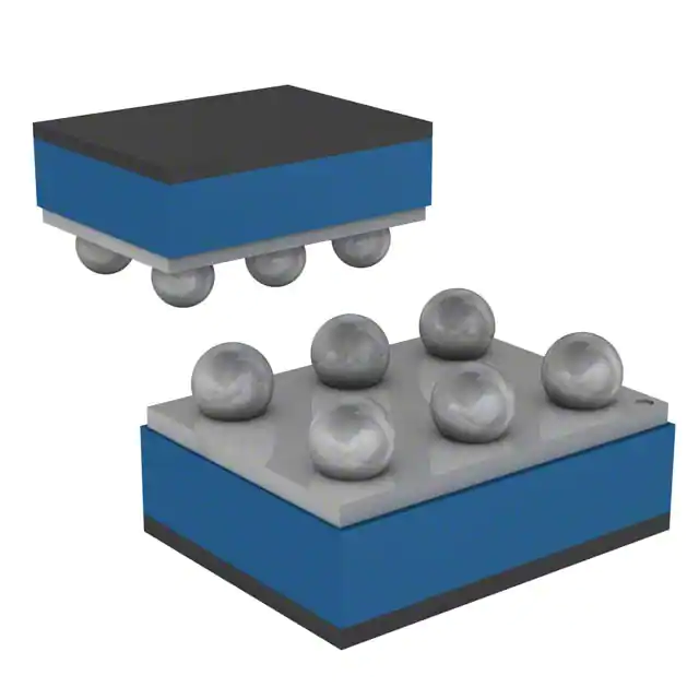
- Part No.:
- CPL-WB-01C2
- Manufacturer:
- STMicroelectronics
- Category:
- RF Directional Coupler
- Package:
- 6-WFBGA, FCBGA
- Datasheet:
-
 CPL-WB-01C2.pdf
- Description:
- IC DIRECTIONAL CPLR FLIPCHIP
- Quantity:
- Payment:

- Shipping:

Inventory:1,974
Please send an inquiry. Send us your inquiry, and we will respond immediately.
Product details
Overview
CPL-WB-01C2 from STMicroelectronics is a wideband directional coupler designed for RF power monitoring in GSM/WCDMA/TD-SCDMA front-end modules, featuring 50 Ω impedance, 824–2025 MHz bandwidth, <0.2 dB insertion loss, 34 dB typical coupling factor, and 25 dB typical directivity. It enables accurate antenna output power sampling in quad-band mobile phone power amplifier modules.
For engineers reviewing the CPL-WB-01C2 datasheet, CPL-WB-01C2 pinout, CPL-WB-01C2 application, or CPL-WB-01C2 equivalent, key selection criteria include coupling ripple (<0.5 dB across bands), ESD robustness (±15 kV air discharge), flip-chip footprint (1700 × 1200 µm), ISO port isolation, and IPD-based glass-substrate RF performance.
Technical Context
The CPL-WB-01C2 implements a four-port passive directional coupler topology using ST's Integrated Passive Device (IPD) process on non-conductive glass substrate, enabling high-frequency stability and minimal parasitic coupling. Its design targets simultaneous coverage of EGSM (824–849 MHz), DCS (1710–1785 MHz), PCS (1850–1910 MHz), and TD-SCDMA (1880–2025 MHz) bands with consistent impedance matching.
It delivers broadband RF signal sampling via dedicated RFIN, RFOUT, CPLD (coupled port), and ISO (isolated port) terminals, with de-embedded measurement reference at bump level. The device operates over −30 °C to +85 °C and supports 35 dBm maximum input power without degradation.
Key Specifications
| Parameter | Value and Actual Design Meaning |
|---|---|
| Frequency Range | 824–2025 MHz: covers all major cellular bands (EGSM, DCS, PCS, TD-SCDMA) in single device |
| Insertion Loss | <0.2 dB typ.: minimizes transmit path attenuation, preserving PA efficiency |
| Coupling Factor | 35–39 dB (824–915 MHz), 28–33 dB (1710–2025 MHz): enables precise low-level RF sampling without external attenuation |
| Directivity | 20–25 dB typ.: ensures high isolation between forward and reverse signal paths for accurate power measurement |
| ESD Rating | ±15 kV air / ±8 kV contact (IEC 61000-4-2 Level 4): eliminates need for external ESD protection in compact RF modules |
| Package Size | 1700 × 1200 µm footprint, <690 µm thickness: fits within tight space constraints of multi-band front-end modules |
| Impedance | 50 Ω nominal on all ports (RFIN, RFOUT, CPLD, ISO): ensures seamless integration into standard 50 Ω RF PCB layouts |
Pinout & Package
Flip-chip package with solder bumps; no leads or wire bonds. Dimensions: 1.700 mm × 1.200 mm × 0.690 mm max. Requires 250–300 µm copper pad diameter and 330 µm stencil opening per bump.
| Pin/Terminal | Circuit Role | Design Meaning |
|---|---|---|
| A1 (RFIN) | RF Input | Main transmit path entry; accepts up to 35 dBm; referenced to ground plane |
| A2 (GND) | Ground | Primary RF return path; must be connected to solid bottom-layer ground plane |
| A3 (GND) | Ground | Secondary ground bump for improved thermal and RF return continuity |
| B1 (RFOUT) | RF Output | Transmit path exit; low-loss continuation to antenna switch or filter |
| B2 (ISO) | Isolated Port | Rejects reverse-traveling signals; used for reflection monitoring or calibration |
| B3 (CPLD) | Coupled Port | Provides sampled forward power (−35 dB typical); feeds power detector or ADC |
Key Features
| Feature | Design Value |
|---|---|
| Wideband Coupling Stability | Coupling ripple ≤0.5 dB across five defined sub-bands - enables single-coupler calibration across full cellular spectrum |
| IPD-on-Glass Construction | Non-conductive glass substrate minimizes dielectric loss and substrate coupling - improves directivity and Q-factor vs. silicon-based passives |
| Integrated ISO Port | Dedicated isolated port provides >20 dB reverse isolation - supports simultaneous forward power and VSWR monitoring |
| Lead-Free Flip-Chip | RoHS-compliant assembly with 100% tested tape-and-reel delivery - eliminates reflow compatibility concerns in high-volume SMT lines |
Applications
| GSM Power Amplifier Module | WCDMA Front-End Module |
|---|---|
Use Scenario: Real-time output power control in dual-mode GSM/EDGE handset PAs. IC Role / Device Role / Timing Role: Directional coupler providing sampled forward RF power to analog power detector IC. Use Value: Enables closed-loop PA bias adjustment with <0.2 dB path loss, maintaining EVM and ACLR compliance across 824–915 MHz band. | Use Scenario: Transmit chain monitoring in 3G WCDMA handsets supporting 1920–2170 MHz UMTS Band I. IC Role / Device Role / Timing Role: Coupler feeding RF power detector for dynamic output power scaling during HSDPA data bursts. Use Value: 28–33 dB coupling factor and 25 dB directivity ensure accurate power readback despite adjacent-band interference. |
| TD-SCDMA Mobile Terminal | Quad-Band Cellular Reference Design |
Use Scenario: Antenna port power sensing in China-specific TD-SCDMA baseband platforms (1880–2025 MHz). IC Role / Device Role / Timing Role: Wideband coupler with ISO port used for both forward power sampling and reflection detection. Use Value: Simultaneous CPLD and ISO outputs support real-time VSWR estimation without adding discrete circulators or switches. | Use Scenario: Single-component RF sampling solution in reference designs targeting global quad-band (850/900/1800/1900 MHz) certification. IC Role / Device Role / Timing Role: Unified coupler replacing multiple narrowband devices in evaluation board layout. Use Value: Reduces BOM count by one component and saves 1.7 mm × 1.2 mm PCB area versus discrete coupler + attenuator combinations. |
Availability
CPL-WB-01C2 is available at Aetrix Electronics and suitable for quad-band power amplifier modules, WCDMA front-end modules, and TD-SCDMA mobile terminal designs requiring stable component supply, high-volume tape-and-reel delivery, and guaranteed lifecycle continuity.
Supply support for CPL-WB-01C2 includes scheduled delivery planning, volume procurement assistance, BOM continuity management, traceable sourcing, and lifecycle availability coordination for OEM customers, industrial embedded developers, connected-device designers, and electronics production programs.
Manufacturer
STMicroelectronics is a global semiconductor leader headquartered in Geneva, Switzerland, delivering intelligent power, analog, MEMS, and microcontroller solutions for automotive, industrial, and consumer applications.
The CPL-WB-01C2 belongs to ST's RF passive portfolio built on IPD technology, specifically engineered for miniaturized, high-performance cellular front-end integration in space-constrained mobile devices.
FAQ
What is the recommended PCB layout for CPL-WB-01C2?
Use coplanar waveguide (CPW) traces: 850 µm line width with 260 µm gap to ground, FR4 substrate (0.8 mm thick), and 10.2 mm line length. Ground plane must be solid on bottom layer; de-embedding reference is at bump level. Avoid vias near coupler pads.
Does CPL-WB-01C2 require external DC blocking capacitors?
No. The device is fully DC-isolated across all ports (RFIN, RFOUT, CPLD, ISO) due to its passive IPD construction on insulating glass substrate. No series capacitors are needed for RF signal path coupling.
Can CPL-WB-01C2 be used for reverse power (reflected signal) measurement?
Yes. The ISO port provides ≥20 dB isolation from RFIN, allowing it to sample reflected signals when RFOUT is connected to antenna. Combined with CPLD port, it enables real-time VSWR calculation without additional components.
What is the maximum RF input power rating?
The absolute maximum RF input power is +35 dBm (3.16 W) at RFIN, specified under continuous-wave conditions at Tamb = 25 °C. Derating is required above +85 °C ambient or under pulsed operation exceeding 10% duty cycle.
CPL-WB-01C2 Specifications
- Product attributes
- Attribute value
- Manufacturer:
- STMicroelectronics
- Series:
- -
- Packaging:
- Tape & Reel (TR)
- Product Status:
- Obsolete
- Coupler Type:
- Standard
- Frequency:
- 824MHz ~ 2.025GHz
- Coupling Factor:
- 34dB
- Applications:
- General Purpose
- Insertion Loss:
- 0.2dB
- Power - Max:
- -
- Isolation:
- -
- Return Loss:
- 15dB
- Supplier Device Package:
- 6-FlipChip
CPL-WB-01C2 FAQ
1.How can I place an order for CPL-WB-01C2 through Aetrix?
Please submit a Request for Quotation (RFQ) for CPL-WB-01C2 on Aetrix. Our sales agent will provide a competitive quotation and guide you through the order confirmation once you accept the terms.
2.Are the price and stock information for CPL-WB-01C2 reliable?
The price and inventory of CPL-WB-01C2 are updated periodically and may fluctuate due to market conditions. Stock and pricing data are typically refreshed every 24 hours. Quotation validity for CPL-WB-01C2 is usually 5 days.
3.What payment methods are accepted for CPL-WB-01C2?
We accept Wire Transfer, PayPal, Credit Card, Western Union, MoneyGram, and Escrow for CPL-WB-01C2 transactions.
Note: Certain payment methods may incur a processing fee.
4.How is shipping managed for CPL-WB-01C2?
CPL-WB-01C2 orders can be shipped via leading logistics carriers, including DHL, UPS, FedEx, TNT, or Registered Mail.
Once your CPL-WB-01C2 order is processed, you will receive an email with the shipment details and tracking number.
Note: Tracking information may take up to 24 hours to appear. Express delivery typically takes 3–5 business days.
5.How can I obtain technical support or documentation for CPL-WB-01C2?
For technical support, including CPL-WB-01C2 datasheets, pinout diagrams, or application guidance, please contact our engineering support team. They can provide detailed documentation and assistance for your CPL-WB-01C2 requirements.
6.How does Aetrix verify that CPL-WB-01C2 is sourced from the original manufacturer or authorized distributors?
All CPL-WB-01C2 products on Aetrix are procured from qualified distributors and authorized channels. Our dedicated quality assurance team conducts strict verification, including traceability checks and, if necessary, third-party testing. This ensures that CPL-WB-01C2 meets industry standards.
7.What is the process for return or replacement of CPL-WB-01C2?
All CPL-WB-01C2 units undergo pre-shipment inspection (PSI). If there is an issue with CPL-WB-01C2, returns or replacements are accepted under the following conditions:
1.Quantity discrepancies, incorrect items, or visible external defects (such as breakage or corrosion), acknowledged by Aetrix.
2.The issue is reported within 90 days of delivery.
3.The CPL-WB-01C2 part is unused and in its original packaging.
Return procedure for CPL-WB-01C2:
1.Submit a request within 90 days.
2.Obtain a Return Material Authorization (RMA) from Aetrix.
CPL-WB-01C2 Tags
.jpg)
-
C0810J5003AHF
TTM Technologies, Inc.
-
C5060J5003AHF
TTM Technologies, Inc.
-
C1517J5003AHF
TTM Technologies, Inc.
-
DC0710J5010AHF
TTM Technologies, Inc.
-
DC2337J5020AHF
TTM Technologies, Inc.
-
C0727J5003AHF
TTM Technologies, Inc.
-
DC2337J5010AHF
TTM Technologies, Inc.

-
0910CF15B0100001E
Johanson Technology Inc.
-
X3C14F1-03S
TTM Technologies, Inc.
-
X4C40K1-20SR
TTM Technologies, Inc.
-
X3C09F1-03S
TTM Technologies, Inc.
.JPG)
-
X3C19F1-03S
TTM Technologies, Inc.
Tech Hub

A practical engineering and sourcing framework covering lifecycle verification, lifetime-buy calculations, replacement qualification, supplier checks and counterfeit-risk controls.

TTL and CMOS logic families differ in thresholds, loading, output drive, power and timing. This engineering guide compares 74HC and 74HCT, calculates noise margins and checks 3.3 V/5 V compatibility.

A practical engineering guide to 3.3V and 5V logic compatibility, input thresholds, resistor dividers, translator ICs, MOSFET level shifting, I2C pull-ups, timing limits and power-sequencing risks.

The 74HC595 uses push-pull logic outputs, while the TPIC6B595 uses 50 V open-drain DMOS sinks for higher-power loads. This guide compares timing, current limits, 3.3 V interfacing, load wiring, thermal…

The 74HC595 converts serial data into eight stable parallel outputs. This guide covers pin functions, shift and storage timing, OE and MR behavior, drive-current limits, cascading, voltage compatibilit…

A technical comparison of level-sensitive latches and edge-triggered flip-flops, covering timing windows, setup and hold limits, master–slave operation, time borrowing, race-through, HDL inference and…

A D latch stores one bit while Enable controls when data can pass. This reference covers gate-level operation, truth tables, transparency, setup and hold timing, LE versus OE, common ICs and practical …

An SR latch stores one bit through cross-coupled feedback. This engineering reference covers NOR and NAND implementations, truth tables, forbidden-state recovery, gated operation, switch debouncing, fa…

Latch circuits retain one bit through feedback. This technical reference covers SR and D latches, truth tables, transparency, timing limits, latch-versus-flip-flop behavior, applications and common log…

An engineering guide to LED driver operation, constant-current and constant-voltage outputs, linear and switching topologies, dimming, IC selection, calculations, replacement compatibility, and fault c…


