
 My Inquiry
 My Account


Texas Instruments CS4210VJG
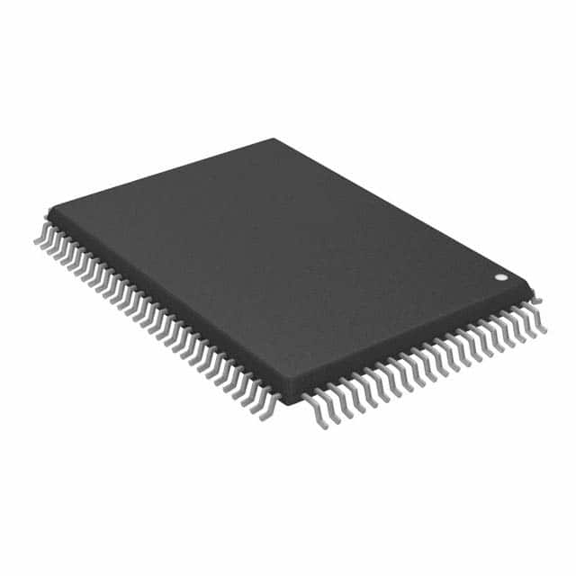
- Part No.:
- CS4210VJG
- Manufacturer:
- Texas Instruments
- Category:
- Controllers
- Package:
- 100-LQFP
- Datasheet:
-
 CS4210VJG.pdf
- Description:
- IC CONTROLLER GEODE OHCI 100LQFP
- Quantity:
- Payment:

- Shipping:

Inventory:3,452
Please send an inquiry. Send us your inquiry, and we will respond immediately.
Product details
Overview
CS4210VJG from National Semiconductor is a PCI-based IEEE 1394 OHCI (Open Host Controller Interface) controller implementing the IEEE 1394 Link Layer per OHCI Specification v1.0, supporting 100/200/400 Mbit/s data transfer, with integrated DMA engines for asynchronous and isochronous traffic, and compatible with Geode CS4103 PHY devices. It targets PC, set-top box, thin client, and WebPAD™ systems requiring high-speed serial interconnect.
For engineers reviewing the CS4210VJG datasheet, CS4210VJG pinout, CS4210VJG application, or CS4210VJG equivalent, this page delivers verified technical context, exact pin functions, FIFO sizing, OHCI register architecture, and validated alternatives for IEEE 1394 host controller selection in embedded and consumer electronics designs.
Technical Context
The CS4210VJG integrates a full PCI bus mastering interface compliant with PCI Rev 2.1, operating at up to 33 MHz with 5V-tolerant I/O. Its DMA engine comprises four dedicated modules: ATDMA for asynchronous transmit, ITDMA for isochronous transmit, RDMA for receive processing, and a shared Transfer Engine handling descriptor movement and byte alignment.
It implements three clock domains: PCI (≤33 MHz), SCLK (49.152 MHz), and SCLK/2 (24.576 MHz). The link layer supports P1394a features including cycle start packet generation, CRC32, and physical request filtering, while the PHY-Link interface connects directly to Geode CS4103 or other IEEE 1394-1995/P1394a Draft 2.0 physical layer devices.
Key Specifications
| Parameter | Value and Actual Design Meaning |
|---|---|
| Data rates | 100/200/400 Mbit/s - Enables compatibility with legacy and high-speed IEEE 1394 devices without protocol translation. |
| PCI interface | PCI Rev 2.1, 5V tolerant, 33 MHz - Integrates directly into standard x86 host platforms without level-shifting circuitry. |
| FIFO memory | 2 KB isochronous TX, 2 KB asynchronous TX, 4 KB RX - Supports sustained real-time audio/video streaming and bursty control data without host CPU intervention. |
| DMA contexts | 8 isochronous TX + 8 isochronous RX contexts - Allows concurrent multi-channel AV streams with independent bandwidth allocation and timing control. |
| Descriptor handling | 128-byte descriptor read in one burst, zero-wait-state bursting - Reduces PCI bus occupancy and improves descriptor fetch latency for high-throughput applications. |
| Physical interface | PHY-Link interface compatible with Geode CS4103 and IEEE 1394-1995/P1394a Draft 2.0 PHYs - Enables modular system design with separate link/physical layer partitioning. |
| Process technology | 0.25 µm CMOS - Provides balanced power efficiency and integration density for cost-sensitive consumer platforms. |
Pinout & Package
CS4210VJG is housed in a 100-pin LQFP (Low-profile Quad Flat Pack) package with 0.5 mm pitch, designed for surface-mount assembly and thermal management in space-constrained consumer electronics enclosures.
| Pin/Terminal | Circuit Role | Design Meaning |
|---|---|---|
| AD[31:0] | PCI address/data multiplexed bus | Carries 32-bit address and data during PCI transactions; requires external latching and timing control per PCI spec. |
| C/BE[3:0]# | PCI command/byte enable | Defines transaction type (I/O, memory, config) and active byte lanes during data phase. |
| FRAME# | PCI frame initiation | Signals start of PCI transaction; asserted by initiator to begin address phase. |
| IRDY# / TRDY# | PCI initiator/target ready | Coordinates data transfer timing: IRDY# from CS4210VJG as initiator, TRDY# from target device. |
| INTA# | PCI interrupt request | Open-drain, level-sensitive interrupt output used for OHCI event signaling (bus reset, DMA completion, errors). |
| DATA[0:7], CTRL[0:1], LREQ, DIRECT, LNKON, LPS, SCLK | PHY-Link interface signals | Direct parallel interface to IEEE 1394 PHY (e.g., CS4103); carries serialized link-layer data, control, and clock synchronization. |
| EECLK / EEDATA | I²C serial EEPROM interface | Supports optional external configuration storage for vendor ID, GUID, and initialization parameters via standard I²C protocol. |
| RST# | Asynchronous reset input | Active-low global reset that clears all internal registers and FIFOs, synchronizing device state with host boot sequence. |
Key Features
| Feature | Design Value |
|---|---|
| OHCI v1.0 compliance | Full implementation of Open Host Controller Interface specification, enabling OS-level driver compatibility (e.g., Windows IEEE 1394 stack, Linux ohci1394). |
| Dynamically re-prioritized services | Hardware arbitration logic adjusts DMA context priority in real time based on packet deadlines and buffer status, ensuring deterministic isochronous delivery. |
| Per-packet FIFO thresholding | Configurable watermark triggers interrupts before FIFO overflow, allowing precise host-side flow control for mixed asynchronous/isochronous traffic. |
| National-specific configuration registers | NSC-defined registers (e.g., nscControl, nscTxThreshold) provide vendor-unique tuning for PHY timing, error recovery, and bandwidth monitoring not available in baseline OHCI. |
| Embedded RAM BIST | On-chip Built-In Self-Test for all SRAM blocks (TxFIFO, RxFIFO, scratchpad) enables production test and field diagnostics without external test equipment. |
Applications
| PC Add-in Card | Set-Top Box |
|---|---|
Use Scenario: Adding IEEE 1394 connectivity to desktop PCs via PCI expansion slot for digital camcorder capture and external storage. IC Role / Device Role / Timing Role: OHCI-compliant host controller managing link-layer packet assembly, DMA transfers, and bus arbitration between host memory and PHY. Use Value: Eliminates need for software-based protocol stacks; offloads 1394 transaction processing from CPU using hardware FIFOs and dual-context DMA engines. | Use Scenario: Enabling high-bandwidth AV streaming between satellite receiver and external digital recorder or home theater system. IC Role / Device Role / Timing Role: Isochronous traffic coordinator with eight independent TX/RX contexts, synchronized to 49.152 MHz SCLK domain for jitter-free audio/video transport. Use Value: Guarantees bounded latency and guaranteed bandwidth for real-time MPEG-2 transport streams without host intervention. |
| Thin Client Terminal | WebPAD™ System |
Use Scenario: Supporting peripheral docking station with IEEE 1394-connected scanners, printers, and biometric sensors in secure enterprise environments. IC Role / Device Role / Timing Role: Asynchronous request/response handler with four concurrent posted writes and eight pending physical responses for low-latency control messaging. Use Value: Enables rapid enumeration and configuration of multiple peripherals via CSR reads/writes while maintaining PCI bus efficiency. | Use Scenario: Integrating IEEE 1394 as primary high-speed I/O for portable multimedia tablet with detachable keyboard and external display dock. IC Role / Device Role / Timing Role: Dual-domain clock manager (PCI + SCLK) coordinating host memory access and link-layer timing across heterogeneous subsystems. Use Value: Synchronizes USB-like plug-and-play functionality with AV-grade isochronous timing using single-chip solution, reducing BOM count and PCB area. |
Equivalent & Alternatives
The following parts are listed as comparable options for similar IEEE 1394 OHCI controller applications.
| Alternative Part | Technical Difference | Application Difference | Selection Advice |
|---|---|---|---|
| Texas Instruments TSB41AB2 | Integrated PHY + link layer in single package; lacks PCI interface and requires external host bridge; no OHCI register set. | Targeted at embedded microcontroller-based systems with limited PCI infrastructure; not drop-in replacement for CS4210VJG. | Select when minimizing component count outweighs need for OHCI software compatibility and PCI-native integration. |
| Agere Systems FW322 | PCI-based OHCI controller with enhanced power management and FireWire 800 (S800) support; larger 144-pin PBGA package; higher gate count. | Designed for next-generation PCs requiring backward-compatible 400 Mbit/s operation plus future S800 readiness. | Choose for new designs needing extended lifecycle support and higher bandwidth headroom beyond IEEE 1394-1995. |
Compared with TSB41AB2 and FW322, CS4210VJG provides strict OHCI v1.0 register compatibility and optimized 100–400 Mbit/s performance in a compact LQFP package, making it ideal for cost-sensitive, space-constrained consumer platforms where proven driver support and minimal external components are critical.
Availability
CS4210VJG is available at Aetrix Electronics and suitable for PC add-in cards, set-top boxes, thin client terminals, and WebPAD™ systems requiring stable component supply and long-term industrial availability.
Supply support for CS4210VJG includes scheduled delivery planning, volume procurement assistance, BOM continuity management, traceable sourcing, and lifecycle availability coordination for OEM customers, industrial embedded developers, connected-device designers, and electronics production programs.
Manufacturer
National Semiconductor was a U.S.-based semiconductor company specializing in analog, interface, and mixed-signal ICs, acquired by Texas Instruments in 2011.
The Geode™ product line-including CS4210VJG-was engineered for highly integrated, low-power x86-compatible computing platforms targeting thin clients, set-top boxes, and portable multimedia devices.
FAQ
What is the primary function of the CS4210VJG in a system architecture?
The CS4210VJG serves as a PCI-based IEEE 1394 OHCI-compliant host controller, implementing the link layer protocol and managing DMA transfers for both asynchronous and isochronous traffic. It bridges the PCI bus to the IEEE 1394 physical layer, enabling high-speed serial communication up to 400 Mbit/s in PCs, set-top boxes, and WebPAD™ systems. Its role is strictly defined by the OHCI v1.0 specification and does not include PHY functionality.
Does the CS4210VJG integrate an IEEE 1394 physical layer?
No, the CS4210VJG does not integrate a physical layer. It provides a dedicated PHY-Link interface compatible with external IEEE 1394 PHY devices such as the Geode CS4103 or other P1394a-compliant transceivers. This separation allows flexible system design where link-layer and physical-layer functions are implemented in discrete ICs, reducing thermal coupling and enabling PHY upgrades independent of the controller.
What clock domains does the CS4210VJG operate in, and why are they significant?
The CS4210VJG operates in three distinct clock domains: PCI (≤33 MHz), SCLK (49.152 MHz), and SCLK/2 (24.576 MHz). This separation isolates high-speed link-layer timing from host bus timing, preventing jitter propagation from the PCI bus into isochronous audio/video streams. The SCLK domain precisely matches IEEE 1394 cycle timing requirements, ensuring deterministic packet transmission and reception essential for real-time AV applications.
How does the CS4210VJG handle isochronous data transfers compared to asynchronous ones?
The CS4210VJG dedicates separate DMA engines-ITDMA for isochronous transmit and RDMA for isochronous receive-with eight configurable contexts each. Isochronous transfers use fixed-bandwidth, time-division-multiplexed channels synchronized to the 49.152 MHz SCLK domain, guaranteeing latency and throughput. Asynchronous transfers use ATDMA with retry logic and acknowledgment handling, prioritizing reliability over timing determinism. Both paths feed into segregated FIFOs (2 KB TX, 4 KB RX) to prevent resource contention.
Is the CS4210VJG compatible with modern operating systems and drivers?
Yes, the CS4210VJG implements the full OHCI v1.0 register set and behavior, ensuring compatibility with standard IEEE 1394 host controller drivers in Windows (e.g., WinXP/Win7 1394 stack), Linux (ohci1394 kernel module), and legacy real-time OSes. Its register layout, interrupt semantics, and DMA descriptor format match the OHCI specification exactly, enabling plug-and-play support without custom driver development for CS4210VJG-based designs.
CS4210VJG Specifications
- Product attributes
- Attribute value
- Manufacturer:
- Texas Instruments
- Package/Case:
- 100-LQFP
- Programmable:
- Not Verified
- Protocol:
- IEEE 1394
- Function:
- Controller
- Interface:
- PCI
- Standards:
- IEEE 1394-1995, OHCI
- Voltage - Supply:
- 3V ~ 3.6V
- Current - Supply:
- 80mA
- Operating Temperature:
- 0°C ~ 70°C
- Supplier Device Package:
- 100-QFP (14x14)
- Grade:
- -
- Qualification:
- -
CS4210VJG FAQ
1.How can I place an order for CS4210VJG through Aetrix?
Please submit a Request for Quotation (RFQ) for CS4210VJG on Aetrix. Our sales agent will provide a competitive quotation and guide you through the order confirmation once you accept the terms.
2.Are the price and stock information for CS4210VJG reliable?
The price and inventory of CS4210VJG are updated periodically and may fluctuate due to market conditions. Stock and pricing data are typically refreshed every 24 hours. Quotation validity for CS4210VJG is usually 5 days.
3.What payment methods are accepted for CS4210VJG?
We accept Wire Transfer, PayPal, Credit Card, Western Union, MoneyGram, and Escrow for CS4210VJG transactions.
Note: Certain payment methods may incur a processing fee.
4.How is shipping managed for CS4210VJG?
CS4210VJG orders can be shipped via leading logistics carriers, including DHL, UPS, FedEx, TNT, or Registered Mail.
Once your CS4210VJG order is processed, you will receive an email with the shipment details and tracking number.
Note: Tracking information may take up to 24 hours to appear. Express delivery typically takes 3–5 business days.
5.How can I obtain technical support or documentation for CS4210VJG?
For technical support, including CS4210VJG datasheets, pinout diagrams, or application guidance, please contact our engineering support team. They can provide detailed documentation and assistance for your CS4210VJG requirements.
6.How does Aetrix verify that CS4210VJG is sourced from the original manufacturer or authorized distributors?
All CS4210VJG products on Aetrix are procured from qualified distributors and authorized channels. Our dedicated quality assurance team conducts strict verification, including traceability checks and, if necessary, third-party testing. This ensures that CS4210VJG meets industry standards.
7.What is the process for return or replacement of CS4210VJG?
All CS4210VJG units undergo pre-shipment inspection (PSI). If there is an issue with CS4210VJG, returns or replacements are accepted under the following conditions:
1.Quantity discrepancies, incorrect items, or visible external defects (such as breakage or corrosion), acknowledged by Aetrix.
2.The issue is reported within 90 days of delivery.
3.The CS4210VJG part is unused and in its original packaging.
Return procedure for CS4210VJG:
1.Submit a request within 90 days.
2.Obtain a Return Material Authorization (RMA) from Aetrix.
CS4210VJG Tags

-
PTN5150AHXMP
NXP Semiconductors

-
USB3740B-AI9-TR
Microchip Technology

-
USB3740B-AI2-TR
Microchip Technology

-
USB3300-EZK-TR
Microchip Technology
-
USB3300-EZK
Microchip Technology

-
FUSB340TMX
onsemi

-
FUSB302BMPX
onsemi

-
DP83826IRHBR
Texas Instruments

-
MCP2518FDT-E/QBB
Microchip Technology
-
FUSB302MPX
onsemi

-
MCP2518FDT-E/SL
Microchip Technology

-
FT260Q-R
FTDI, Future Technology Devices International Ltd
Tech Hub

A practical engineering guide to 3.3V and 5V logic compatibility, input thresholds, resistor dividers, translator ICs, MOSFET level shifting, I2C pull-ups, timing limits and power-sequencing risks.

The 74HC595 uses push-pull logic outputs, while the TPIC6B595 uses 50 V open-drain DMOS sinks for higher-power loads. This guide compares timing, current limits, 3.3 V interfacing, load wiring, thermal…

The 74HC595 converts serial data into eight stable parallel outputs. This guide covers pin functions, shift and storage timing, OE and MR behavior, drive-current limits, cascading, voltage compatibilit…

A technical comparison of level-sensitive latches and edge-triggered flip-flops, covering timing windows, setup and hold limits, master–slave operation, time borrowing, race-through, HDL inference and…

A D latch stores one bit while Enable controls when data can pass. This reference covers gate-level operation, truth tables, transparency, setup and hold timing, LE versus OE, common ICs and practical …

An SR latch stores one bit through cross-coupled feedback. This engineering reference covers NOR and NAND implementations, truth tables, forbidden-state recovery, gated operation, switch debouncing, fa…

Latch circuits retain one bit through feedback. This technical reference covers SR and D latches, truth tables, transparency, timing limits, latch-versus-flip-flop behavior, applications and common log…

An engineering guide to LED driver operation, constant-current and constant-voltage outputs, linear and switching topologies, dimming, IC selection, calculations, replacement compatibility, and fault c…

Operational amplifier guide covering op amp basics, feedback, ideal vs real op amps, common configurations, buffer circuits, offset, bias current, gain-bandwidth, slew rate, rail-to-rail limits and sel…

Jumper cables guide covering safe connection order, red and black clamp placement, final ground connection, cable gauge, length, clamp quality, copper vs CCA cables, jump starter comparison and battery…


