
 My Inquiry
 My Account


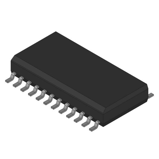
onsemi CS5112YDWFR24G
- Part No.:
- CS5112YDWFR24G
- Manufacturer:
- onsemi
- Package:
- -
- Datasheet:
-
 CS5112YDWFR24G.pdf
- Description:
- IC REG
- Quantity:
- Payment:

- Shipping:

Inventory:942
Please send an inquiry. Send us your inquiry, and we will respond immediately.
Product details
Overview
CS5112YDWFR24G from onsemi is a dual-output power management IC integrating a 5.0 V ±2% linear regulator (100 mA), a 1.4 A current-mode PWM switching regulator, watchdog timer, active-low RESET with programmable delay, and ENABLE control. It operates from 5.0 V to 26 V input, supports boost topology, and delivers stable bias for microcontrollers in automotive body electronics and industrial control modules.
For engineers reviewing the CS5112YDWFR24G datasheet, pinout, applications, or equivalent options, key selection considerations include its dual-regulator architecture, externally programmable watchdog/RESET timing via CDelay/RBIAS, selectable feedback inputs (VFB1/VFB2), thermal shutdown at 160°C, and SOIC-24 Pb-free package with fused leads.
Technical Context
The CS5112YDWFR24G implements a current-mode PWM controller with adjustable oscillator (80–120 kHz), internal 1.4 A NPN switch, and antisaturation control. Its error amplifier supports two feedback inputs (VFB1/VFB2) referenced to 1.25 V, enabling dynamic output voltage selection via the SELECT pin.
The integrated 5.0 V linear regulator uses a composite pass transistor (Q1–Q3), bandgap reference, and error amplifier with 1.2 V typical dropout at 100 mA. Supervisory functions include a falling-edge-triggered watchdog (tWDI = 1.353 × CDelay × RBIAS), POR delay (tPOR = same RC time constant), and RESET output that toggles low during undervoltage or watchdog timeout.
Key Specifications
| Parameter | Value and Actual Design Meaning |
|---|---|
| Linear Output | 5.0 V ±2% at 100 mA load; provides clean, low-noise bias for MCU cores and peripherals. |
| Switching Output | 1.4 A peak internal NPN switch; enables high-efficiency boost conversion up to 26 V input. |
| Operating Input Range | 5.0 V to 26 V DC; supports wide automotive battery range including load dump transients up to 40 V. |
| Watchdog & RESET Timing | Programmable via single RC network (CDelay + RBIAS); tWDI/tPOR = 1.353 × CDelay × RBIAS (e.g., 6.25–11 ms). |
| Thermal Protection | Overtemperature limiter activates at 160°C die temperature; reduces VLIN to throttle power dissipation. |
| Feedback Flexibility | VFB1 and VFB2 both regulated to 1.25 V; SELECT pin chooses between them for dual-output voltage programming. |
| Package | SOIC-24 (Case 751E); Pb-free, internally fused leads, RJA = 55°C/W, RJC = 9°C/W. |
Pinout & Package
CS5112YDWFR24G is housed in a 24-pin SOIC package (Case 751E) with eight GND pins (pins 5,6,7,8,17,18,19,20) for thermal and noise performance. Internally fused leads enhance reliability under surge conditions.
| Pin/Terminal | Circuit Role | Design Meaning |
|---|---|---|
| VIN (Pin 1) | Switching regulator supply input | Provides base drive to internal NPN switch; must be ≥5.0 V for operation. |
| VSW (Pin 4) | Switch collector output | Drives external inductor in boost configuration; withstands 54 V transient. |
| VLIN (Pin 22) | 5.0 V linear regulator output | Supplies MCU core logic and internal circuitry; dropout = 1.2 V @ 100 mA. |
| VREG (Pin 23) | Linear regulator input | Accepts 6.6–26 V unregulated input; powers linear section and internal bias. |
| ENABLE (Pin 24) | Switching regulator enable/disable | Logic-high disables PWM section only; linear regulator remains active. |
| WDI (Pin 14) | Watchdog input | Falling-edge triggered; timeout resets system if pulse not received within tWDI. |
| RESET (Pin 16) | Active-low reset output | Pulses low during POR or watchdog failure; sinks 5 mA; valid down to VLIN = 1.0 V. |
| SELECT (Pin 11) | Feedback input selector | Open = VFB2 active; grounded = VFB1 active; enables dual-voltage boost regulation. |
Key Features
| Feature | Design Value |
|---|---|
| Dual-regulator integration | Combines 5.0 V/100 mA LDO and 1.4 A PWM switcher in one SOIC-24, reducing BOM count and PCB area vs. discrete solutions. |
| Programmable supervision | Single RC network (CDelay + RBIAS) sets both Power-On Reset delay and watchdog timeout - simplifies timing design and component count. |
| Load-dump robustness | Withstands 40 V transient on VIN and 54 V on VSW; meets automotive ISO 7637-2 pulse 5a requirements without external clamping. |
| Thermal and current protection | Internally limits linear and switching output currents; die temperature limit at 160°C prevents thermal runaway in enclosed environments. |
| Flexible feedback architecture | VFB1/VFB2 inputs both referenced to 1.25 V with 1.206–1.294 V tolerance; SELECT pin allows runtime switching between two regulated outputs. |
Applications
| Automotive Body Control Module (BCM) | Industrial PLC I/O Power Supply |
|---|---|
|
Use Scenario: Powering microcontroller, CAN transceiver, and sensor interface circuitry in a vehicle door module. IC Role / Device Role / Timing Role: CS5112YDWFR24G supplies 5.0 V to MCU core and generates boosted 18 V for window motor drivers using boost topology. Use Value: Integrated watchdog and RESET eliminate need for external supervisor IC; load-dump tolerance avoids TVS diodes on VIN. |
Use Scenario: Providing isolated 5.0 V logic rail and programmable 16–18 V analog front-end supply in modular PLC backplane. IC Role / Device Role / Timing Role: CS5112YDWFR24G's SELECT pin dynamically switches between VFB1/VFB2 to adjust boost output based on I/O card type. Use Value: Single IC replaces dual regulators + supervisor + timer; RC-programmable RESET ensures deterministic startup sequencing. |
| Smart Lighting Controller | Telematics Power Management |
|
Use Scenario: Driving LED driver ICs and MCU in an adaptive headlamp ECU requiring stable 5.0 V and >12 V auxiliary rail. IC Role / Device Role / Timing Role: CS5112YDWFR24G's 1.4 A switcher delivers 16 V to LED buck controllers; linear regulator powers safety-critical MCU. Use Value: Thermal limiting prevents overheating during extended high-brightness operation; watchdog guards against firmware lockup. |
Use Scenario: Powering GPS/GNSS receiver, cellular modem, and host processor in automotive telematics unit with battery backup. IC Role / Device Role / Timing Role: CS5112YDWFR24G monitors main battery voltage via VLIN and issues RESET if voltage drops below 4.25 V (typical). Use Value: Active-low RESET with 1.0 V minimum operating threshold ensures reliable brownout detection even during cranking. |
Equivalent & Alternatives
The following parts are listed as comparable options for similar dual-output power management applications.
| Alternative Part | Technical Difference | Application Difference | Selection Advice |
|---|---|---|---|
| LM2678SD-5.0/NOPB | Single 5.0 V buck regulator (5 A), no linear regulator, no watchdog/RESET, no SELECT feedback option. | Lacks integrated supervision and dual-rail capability; requires external supervisor and LDO for similar functionality. | Choose when only high-current 5.0 V buck is needed and supervision is handled elsewhere. |
| TPS54340DDAR | 42 V, 3.5 A buck regulator with enable and power-good, but no linear regulator, watchdog, or RESET generator. | No built-in 5.0 V LDO or system-level reset logic; cannot replace CS5112YDWFR24G's supervisory functions. | Select for higher-efficiency, higher-current buck-only designs where external reset IC is acceptable. |
Compared with LM2678SD-5.0/NOPB and TPS54340DDAR, the CS5112YDWFR24G uniquely integrates linear regulation, switching regulation, watchdog, and programmable RESET in one SOIC-24 package - eliminating four external components while ensuring deterministic power-up and fault recovery in safety-critical embedded systems.
Availability
CS5112YDWFR24G is available at Aetrix Electronics and suitable for automotive body electronics, industrial PLCs, smart lighting controllers, and telematics modules requiring stable component supply, long-term lifecycle support, and AEC-Q100-aligned reliability.
Supply support for CS5112YDWFR24G includes scheduled delivery planning, volume procurement assistance, BOM continuity management, traceable sourcing, and lifecycle availability coordination for OEM customers, industrial embedded developers, connected-device designers, and electronics production programs.
Manufacturer
onsemi (formerly ON Semiconductor) is a global semiconductor supplier focused on energy-efficient innovation for automotive, industrial, cloud, and IoT applications.
The CS5112YDWFR24G belongs to onsemi's automotive-grade power management IC family, designed specifically for robust, integrated power and supervision in harsh-environment embedded control systems.
FAQ
What is the maximum input voltage rating for CS5112YDWFR24G?
The CS5112YDWFR24G supports a DC input voltage range of 5.0 V to 26 V on VIN and VREG. It withstands peak transients up to 40 V on VIN (load dump per ISO 7637-2) and 54 V on VSW, making it suitable for 12 V and 24 V automotive systems. Exceeding these ratings may cause permanent damage.
How does the watchdog timer in CS5112YDWFR24G operate?
The CS5112YDWFR24G watchdog monitors the WDI pin for falling edges. If no edge occurs within the time set by CDelay and RBIAS (tWDI = 1.353 × CDelay × RBIAS), it triggers a repeating RESET pulse train until a valid watchdog signal resumes. The nominal pulse frequency is fRESET = 1/(2 × tWDI).
Can CS5112YDWFR24G be used in buck topology?
No - the CS5112YDWFR24G's internal NPN switch and block diagram are configured exclusively for boost topology. Its VSW pin is the collector output, requiring external inductor between VIN and VSW. Buck operation would require PNP or high-side NMOS switching not supported by this device.
What is the purpose of the SELECT pin on CS5112YDWFR24G?
The SELECT pin on CS5112YDWFR24G chooses between two internal feedback references: open = VFB2 active, grounded = VFB1 active. Both VFB1 and VFB2 are regulated to 1.25 V, allowing dynamic selection of two different boost output voltages using external resistor dividers - useful for multi-rail systems.
Does CS5112YDWFR24G provide overcurrent protection on the linear regulator output?
Yes - the CS5112YDWFR24G includes internal current limiting on the VLIN output, with a typical trip point of 120 mA. This protects the linear regulator from damage during short-circuit or overload conditions, complementing the 1.4 A switcher current limit and thermal shutdown.
CS5112YDWFR24G Specifications
- Product attributes
- Attribute value
- Manufacturer:
- onsemi
- Series:
- *
- Package/Case:
- -
- Packaging:
- Bulk
- Product Status:
- Active
- Function:
- -
- Output Configuration:
- -
- Topology:
- -
- Output Type:
- -
- Number of Outputs:
- -
- Voltage - Input (Min):
- -
- Voltage - Input (Max):
- -
- Voltage - Output (Min/Fixed):
- -
- Voltage - Output (Max):
- -
- Current - Output:
- -
- Frequency - Switching:
- -
- Synchronous Rectifier:
- -
- Operating Temperature:
- -
- Grade:
- -
- Qualification:
- -
- Mounting Type:
- -
- Supplier Device Package:
- -
CS5112YDWFR24G FAQ
1.How can I place an order for CS5112YDWFR24G through Aetrix?
Please submit a Request for Quotation (RFQ) for CS5112YDWFR24G on Aetrix. Our sales agent will provide a competitive quotation and guide you through the order confirmation once you accept the terms.
2.Are the price and stock information for CS5112YDWFR24G reliable?
The price and inventory of CS5112YDWFR24G are updated periodically and may fluctuate due to market conditions. Stock and pricing data are typically refreshed every 24 hours. Quotation validity for CS5112YDWFR24G is usually 5 days.
3.What payment methods are accepted for CS5112YDWFR24G?
We accept Wire Transfer, PayPal, Credit Card, Western Union, MoneyGram, and Escrow for CS5112YDWFR24G transactions.
Note: Certain payment methods may incur a processing fee.
4.How is shipping managed for CS5112YDWFR24G?
CS5112YDWFR24G orders can be shipped via leading logistics carriers, including DHL, UPS, FedEx, TNT, or Registered Mail.
Once your CS5112YDWFR24G order is processed, you will receive an email with the shipment details and tracking number.
Note: Tracking information may take up to 24 hours to appear. Express delivery typically takes 3–5 business days.
5.How can I obtain technical support or documentation for CS5112YDWFR24G?
For technical support, including CS5112YDWFR24G datasheets, pinout diagrams, or application guidance, please contact our engineering support team. They can provide detailed documentation and assistance for your CS5112YDWFR24G requirements.
6.How does Aetrix verify that CS5112YDWFR24G is sourced from the original manufacturer or authorized distributors?
All CS5112YDWFR24G products on Aetrix are procured from qualified distributors and authorized channels. Our dedicated quality assurance team conducts strict verification, including traceability checks and, if necessary, third-party testing. This ensures that CS5112YDWFR24G meets industry standards.
7.What is the process for return or replacement of CS5112YDWFR24G?
All CS5112YDWFR24G units undergo pre-shipment inspection (PSI). If there is an issue with CS5112YDWFR24G, returns or replacements are accepted under the following conditions:
1.Quantity discrepancies, incorrect items, or visible external defects (such as breakage or corrosion), acknowledged by Aetrix.
2.The issue is reported within 90 days of delivery.
3.The CS5112YDWFR24G part is unused and in its original packaging.
Return procedure for CS5112YDWFR24G:
1.Submit a request within 90 days.
2.Obtain a Return Material Authorization (RMA) from Aetrix.
CS5112YDWFR24G Tags
-
TPS562201DDCR
Texas Instruments

-
MC34063ABD-TR
STMicroelectronics
-
TPS561201DDCR
Texas Instruments

-
MC33063ADR
Texas Instruments
-
MC34063ADR
Texas Instruments

-
TPS560200DBVR
Texas Instruments
-
AP3012KTR-G1
Diodes Incorporated
-
TLV61048DBVR
Texas Instruments
-
AZ34063UMTR-G1
Diodes Incorporated
-
TPS562200DDCR
Texas Instruments
-
AP62300TWU-7
Diodes Incorporated
-
MC34063EBD-TR
STMicroelectronics
Tech Hub

Counterfeit components can hide behind convincing markings and passing basic function tests. This engineering reference covers source traceability, external inspection, X-ray, XRF, electrical testing, …

A practical engineering and sourcing framework covering lifecycle verification, lifetime-buy calculations, replacement qualification, supplier checks and counterfeit-risk controls.

TTL and CMOS logic families differ in thresholds, loading, output drive, power and timing. This engineering guide compares 74HC and 74HCT, calculates noise margins and checks 3.3 V/5 V compatibility.

A practical engineering guide to 3.3V and 5V logic compatibility, input thresholds, resistor dividers, translator ICs, MOSFET level shifting, I2C pull-ups, timing limits and power-sequencing risks.

The 74HC595 uses push-pull logic outputs, while the TPIC6B595 uses 50 V open-drain DMOS sinks for higher-power loads. This guide compares timing, current limits, 3.3 V interfacing, load wiring, thermal…

The 74HC595 converts serial data into eight stable parallel outputs. This guide covers pin functions, shift and storage timing, OE and MR behavior, drive-current limits, cascading, voltage compatibilit…

A technical comparison of level-sensitive latches and edge-triggered flip-flops, covering timing windows, setup and hold limits, master–slave operation, time borrowing, race-through, HDL inference and…

A D latch stores one bit while Enable controls when data can pass. This reference covers gate-level operation, truth tables, transparency, setup and hold timing, LE versus OE, common ICs and practical …

An SR latch stores one bit through cross-coupled feedback. This engineering reference covers NOR and NAND implementations, truth tables, forbidden-state recovery, gated operation, switch debouncing, fa…

Latch circuits retain one bit through feedback. This technical reference covers SR and D latches, truth tables, transparency, timing limits, latch-versus-flip-flop behavior, applications and common log…


