
 My Inquiry
 My Account


Renesas CS80C286-16
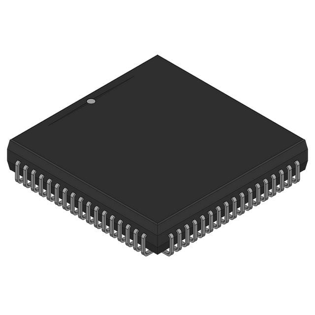
- Part No.:
- CS80C286-16
- Manufacturer:
- Renesas
- Category:
- Microprocessors
- Package:
- 68-LCC (J-Lead)
- Datasheet:
-
 CS80C286-16.pdf
- Description:
- IC MPU 16MHZ 68PLCC
- Quantity:
- Payment:

- Shipping:

Inventory:1,490
Please send an inquiry. Send us your inquiry, and we will respond immediately.
Product details
Overview
CS80C286-16 from Intersil is a static CMOS 16-bit microprocessor with integrated memory management unit (MMU), supporting real and protected virtual address modes, 16 MB physical / 1 GB virtual address space per task, 16 MHz maximum clock frequency, and compatibility with 80C86/80C88 software. It targets embedded industrial control systems requiring deterministic multi-tasking and hardware-enforced memory protection.
For engineers reviewing the CS80C286-16 datasheet, CS80C286-16 pinout, CS80C286-16 application, or CS80C286-16 equivalent, key selection considerations include its 68-pin PLCC package, static CMOS operation enabling DC-to-16 MHz clocking, bus cycle status encoding (S0/S1/M/IO/COD/INTA), BHE/A0 byte/word transfer control, and support for 80287 numeric coprocessor interfacing.
Technical Context
The CS80C286-16 implements a segmented memory architecture with four 16-bit segment registers (CS, DS, SS, ES), a 16-bit instruction pointer, and a 16-bit flags register including IF, TF, DF, IOPL, and PE bits. Its protected virtual address mode uses descriptor tables to map 30-bit virtual addresses into 24-bit physical addresses with four-level privilege protection.
Bus interface logic supports high-bandwidth transfers up to 25 MB/s via 24-bit address bus (A23–A0), 16-bit data bus (D15–D0), BHE-controlled upper-byte enable, and synchronous status signals (S0/S1) decoded with M/IO and COD/INTA to distinguish memory reads, I/O writes, interrupt acknowledges, and instruction fetches.
Key Specifications
| Parameter | Value and Actual Design Meaning |
|---|---|
| Max Clock Frequency | 16 MHz - defines maximum instruction throughput and bus cycle timing; enables full compatibility with 80287 at same speed grade. |
| Operating Voltage | +5 V ±10% - standard TTL-compatible supply; requires 0.1 µF decoupling between VCC pins 30 and 62. |
| Active Current (ICCOP) | 260 mA maximum - determines power supply sizing and thermal design for sustained 16 MHz operation. |
| Standby Current (ICCSB) | 5 mA maximum - enables ultra-low-power sleep states when clock is halted in phase two. |
| Address Space | 16 MB physical / 1 GB virtual per task - supports large-scale real-time OS kernels with task isolation and demand-paged virtual memory. |
| Bus Bandwidth | 25 MB/s - sets peak memory subsystem bandwidth requirement for instruction/data fetch and peripheral I/O. |
| Instruction Set | Superset of 80C86/80C88 - ensures binary compatibility in real mode and source compatibility in protected mode with extended privilege and descriptor instructions. |
Pinout & Package
CS80C286-16 is supplied in a 68-lead plastic leaded chip carrier (PLCC) package, pin-compatible with other CS80C286 variants and designed for surface-mount assembly on industrial PCBs. Thermal and mechanical characteristics align with JEDEC MS-026.
| Pin/Terminal | Circuit Role | Design Meaning |
|---|---|---|
| D15–D0 | Data Bus (I/O) | 16-bit bidirectional data path; high-impedance during bus hold; used for memory/I/O transfers and interrupt vector reads. |
| A23–A0 | Address Bus (O) | 24-bit physical address output; A23–A16 low during I/O cycles; enables 16 MB addressing with byte alignment. |
| BHE | Bus High Enable (O) | Active-low signal indicating valid data on D15–D8; used with A0 to decode word/byte transfers per Intel protocol. |
| S0, S1 | Bus Cycle Status (O) | Two-bit encoded state indicating bus cycle type (e.g., memory read, I/O write, interrupt acknowledge) alongside M/IO and COD/INTA. |
| M/IO | Memory/I/O Select (O) | Active-high distinguishes memory accesses (HIGH) from I/O or interrupt cycles (LOW); critical for peripheral decoding. |
| COD/INTA | Code/Interrupt Acknowledge (O) | High during instruction fetches; low during interrupt acknowledges; synchronizes external interrupt controller handshaking. |
| PEREQ, PEACK | Processor Extension Request/Ack (I/O) | Supports 80287 coprocessor integration: PEREQ requests operand transfer; PEACK confirms data availability on bus. |
| RESET | System Reset (I) | Active-high asynchronous reset; requires >16 clock cycles active; initiates internal initialization and forces known bus state. |
Key Features
| Feature | Design Value |
|---|---|
| Static CMOS Architecture | Enables true DC-to-16 MHz operation with zero minimum frequency constraint and clock-stop capability for debug or power gating. |
| Protected Virtual Address Mode (PVAM) | Hardware-enforced memory protection with four privilege levels, descriptor-based segmentation, and task switching via single instruction (TASK SWITCH). |
| Real Address Mode Compatibility | Full object-code compatibility with 80C86/80C88 software; executes legacy DOS-style applications without modification. |
| Integrated Memory Management Unit (MMU) | Maps 1 GB virtual space per task into 16 MB physical RAM using segment descriptors; eliminates need for external MMU ICs. |
| 25 MB/s High-Bandwidth Bus Interface | Supports fast memory subsystems and burst-capable peripherals; reduces wait-state dependency in real-time control loops. |
Applications
| Industrial PLC Controller | Avionics Data Acquisition Unit |
|---|---|
Use Scenario: Real-time ladder logic execution with deterministic I/O scanning and watchdog supervision across multiple isolated tasks. IC Role / Device Role / Timing Role: Central processing unit managing time-critical control threads, memory-mapped I/O, and fault-tolerant task scheduling. Use Value: Hardware memory protection prevents rogue task corruption of kernel or other task data spaces, ensuring SIL-2 compliance. |
Use Scenario: Sensor fusion system collecting analog/digital inputs from inertial measurement units and environmental sensors under DO-178B constraints. IC Role / Device Role / Timing Role: Deterministic host processor executing certified flight software with strict partitioning between sensor drivers and navigation algorithms. Use Value: Protected mode enables ARINC-653 compliant partitioning-each module runs in dedicated virtual address space with enforced access rights. |
| Medical Imaging Subsystem | Ruggedized Military Terminal |
Use Scenario: Embedded image preprocessing pipeline handling DICOM-compliant frame buffering, histogram equalization, and compression before display. IC Role / Device Role / Timing Role: High-throughput compute engine interfacing with dual-port video RAM and custom ASIC co-processors via local bus. Use Value: 25 MB/s bus bandwidth sustains real-time pixel streaming; 16 MB physical address space accommodates large frame buffers. |
Use Scenario: Field-deployable C4I terminal running secure comms stack, map rendering, and cryptographic services in harsh EMI environments. IC Role / Device Role / Timing Role: Trusted execution platform enforcing separation between crypto keys (ring 0), UI (ring 2), and network stack (ring 3). Use Value: Four-level privilege model isolates security-critical operations from user-facing components, meeting NSA Type 1 requirements. |
Equivalent & Alternatives
The following parts are listed as comparable options for similar 16-bit microprocessor applications.
| Alternative Part | Technical Difference | Application Difference | Selection Advice |
|---|---|---|---|
| IG80C286-16 | Same core, -40°C to +85°C industrial temperature range; PGA package instead of PLCC; identical electrical specs and pinout mapping. | Preferred for conduction-cooled chassis or vibration-prone environments where PGA mechanical stability outweighs PLCC solder joint reliability concerns. | Select IG80C286-16 when board-level shock/vibration exceeds IPC-TR-579 Class 3 and thermal cycling demands ceramic PGA hermeticity. |
| CS80C286-20 | Same PLCC package and feature set, but rated for 20 MHz max clock; higher ICCOP (310 mA) and tighter timing margins on READY/PEREQ setup/hold. | Used where throughput headroom is required for future firmware upgrades or additional ISR load without changing PCB layout. | Choose CS80C286-20 only if system timing analysis confirms all bus peripherals meet 20 MHz cycle times; otherwise CS80C286-16 offers optimal power/performance trade-off. |
Compared with IG80C286-16, CS80C286-16 offers lower-cost surface-mount assembly and reduced board area; compared with CS80C286-20, it delivers 18% lower active power at equivalent workload while maintaining full instruction and pin compatibility.
Availability
CS80C286-16 is available at Aetrix Electronics and suitable for industrial PLC controllers, avionics data acquisition units, and medical imaging subsystems requiring stable component supply across extended product lifecycles.
Supply support for CS80C286-16 includes scheduled delivery planning, volume procurement assistance, BOM continuity management, traceable sourcing, and lifecycle availability coordination for OEM customers, industrial embedded developers, connected-device designers, and electronics production programs.
Manufacturer
Intersil Corporation was a U.S.-based semiconductor company specializing in high-performance analog and mixed-signal ICs, later acquired by Renesas Electronics in 2017. Known for robust industrial-grade microprocessors and precision power management solutions.
The 80C286 family was engineered to deliver NMOS 80286 functionality with static CMOS efficiency, targeting mission-critical embedded systems needing long-term availability, wide temperature operation, and hardware memory protection without external MMUs.
FAQ
What is the operating temperature range for CS80C286-16?
The CS80C286-16 is specified for commercial temperature operation from 0°C to +70°C. This range is validated per the Intersil FN2947 datasheet Rev.3.00 and applies to the PLCC package variant marked "CS". Units intended for industrial or military use carry different prefixes (IS/IG/5962-) and wider temperature grades.
Does CS80C286-16 support the 80287 numeric coprocessor?
Yes, CS80C286-16 fully supports the 80287 numeric data coprocessor via dedicated PEREQ and PEACK signals, as documented in the FN2947 datasheet Section 4. These pins enable synchronized operand transfers and exception handling required for floating-point math acceleration in protected mode applications.
How does CS80C286-16 handle memory protection in protected virtual address mode?
In protected virtual address mode, CS80C286-16 enforces memory protection using descriptor tables stored in memory, with four privilege levels (rings 0–3), segment limit checking, and access rights validation on every memory reference. The hardware MMU traps violations into processor exceptions, preventing unauthorized code or data access without software intervention.
Can CS80C286-16 operate at frequencies below 16 MHz?
Yes, CS80C286-16 is a static CMOS device and operates from DC to 16 MHz. Clock can be stopped indefinitely in phase two to reduce ICCSB to ≤5 mA, making it suitable for low-power wake-on-interrupt designs. All timing parameters scale linearly with clock period per FN2947 Section 6.
What package type is used for CS80C286-16?
CS80C286-16 is supplied in a 68-lead plastic leaded chip carrier (PLCC) package, identified by ordering code N68.95 in the Intersil FN2947 datasheet. This surface-mount package features J-leads, a 0.050" lead pitch, and is compatible with standard reflow soldering profiles for industrial PCB assembly.
CS80C286-16 Specifications
- Product attributes
- Attribute value
- Manufacturer:
- Renesas
- Package/Case:
- 68-LCC (J-Lead)
- Series:
- -
- Packaging:
- Tube
- Product Status:
- Obsolete
- Core Processor:
- 80C286
- Number of Cores/Bus Width:
- 1 Core, 16-Bit
- Speed:
- 16MHz
- Co-Processors/DSP:
- Math Engine; 80C287
- RAM Controllers:
- -
- Graphics Acceleration:
- No
- Display & Interface Controllers:
- -
- Ethernet:
- -
- SATA:
- -
- USB:
- -
- Voltage - I/O:
- 5.0V
- Operating Temperature:
- 0°C ~ 70°C (TA)
- Grade:
- -
- Qualification:
- -
- Security Features:
- -
- Mounting Type:
- Surface Mount
- Supplier Device Package:
- 68-PLCC (24.23x24.23)
- Additional Interfaces:
- -
CS80C286-16 FAQ
1.How can I place an order for CS80C286-16 through Aetrix?
Please submit a Request for Quotation (RFQ) for CS80C286-16 on Aetrix. Our sales agent will provide a competitive quotation and guide you through the order confirmation once you accept the terms.
2.Are the price and stock information for CS80C286-16 reliable?
The price and inventory of CS80C286-16 are updated periodically and may fluctuate due to market conditions. Stock and pricing data are typically refreshed every 24 hours. Quotation validity for CS80C286-16 is usually 5 days.
3.What payment methods are accepted for CS80C286-16?
We accept Wire Transfer, PayPal, Credit Card, Western Union, MoneyGram, and Escrow for CS80C286-16 transactions.
Note: Certain payment methods may incur a processing fee.
4.How is shipping managed for CS80C286-16?
CS80C286-16 orders can be shipped via leading logistics carriers, including DHL, UPS, FedEx, TNT, or Registered Mail.
Once your CS80C286-16 order is processed, you will receive an email with the shipment details and tracking number.
Note: Tracking information may take up to 24 hours to appear. Express delivery typically takes 3–5 business days.
5.How can I obtain technical support or documentation for CS80C286-16?
For technical support, including CS80C286-16 datasheets, pinout diagrams, or application guidance, please contact our engineering support team. They can provide detailed documentation and assistance for your CS80C286-16 requirements.
6.How does Aetrix verify that CS80C286-16 is sourced from the original manufacturer or authorized distributors?
All CS80C286-16 products on Aetrix are procured from qualified distributors and authorized channels. Our dedicated quality assurance team conducts strict verification, including traceability checks and, if necessary, third-party testing. This ensures that CS80C286-16 meets industry standards.
7.What is the process for return or replacement of CS80C286-16?
All CS80C286-16 units undergo pre-shipment inspection (PSI). If there is an issue with CS80C286-16, returns or replacements are accepted under the following conditions:
1.Quantity discrepancies, incorrect items, or visible external defects (such as breakage or corrosion), acknowledged by Aetrix.
2.The issue is reported within 90 days of delivery.
3.The CS80C286-16 part is unused and in its original packaging.
Return procedure for CS80C286-16:
1.Submit a request within 90 days.
2.Obtain a Return Material Authorization (RMA) from Aetrix.
CS80C286-16 Tags

-
AT91SAM9260B-CU-999
Microchip Technology
-
AT91SAM9G25-CU
Microchip Technology

-
ATSAMA5D27C-CU
Microchip Technology
-
AT91SAM9X35-CU
Microchip Technology
-
AT91SAM9X25-CU
Microchip Technology

-
MCIMX6Y2CVM08AB
NXP Semiconductors
.JPG)
-
AM3352BZCZ100
Texas Instruments
-
AT91SAM9260B-CU
Microchip Technology

-
AT91SAM9260B-QU
Microchip Technology

-
ATSAMA5D31A-CU
Microchip Technology
-
AT91SAM9G20B-CU-999
Microchip Technology
-
MCIMX6Y2CVM05AB
NXP Semiconductors
Tech Hub

TTL and CMOS logic families differ in thresholds, loading, output drive, power and timing. This engineering guide compares 74HC and 74HCT, calculates noise margins and checks 3.3 V/5 V compatibility.

A practical engineering guide to 3.3V and 5V logic compatibility, input thresholds, resistor dividers, translator ICs, MOSFET level shifting, I2C pull-ups, timing limits and power-sequencing risks.

The 74HC595 uses push-pull logic outputs, while the TPIC6B595 uses 50 V open-drain DMOS sinks for higher-power loads. This guide compares timing, current limits, 3.3 V interfacing, load wiring, thermal…

The 74HC595 converts serial data into eight stable parallel outputs. This guide covers pin functions, shift and storage timing, OE and MR behavior, drive-current limits, cascading, voltage compatibilit…

A technical comparison of level-sensitive latches and edge-triggered flip-flops, covering timing windows, setup and hold limits, master–slave operation, time borrowing, race-through, HDL inference and…

A D latch stores one bit while Enable controls when data can pass. This reference covers gate-level operation, truth tables, transparency, setup and hold timing, LE versus OE, common ICs and practical …

An SR latch stores one bit through cross-coupled feedback. This engineering reference covers NOR and NAND implementations, truth tables, forbidden-state recovery, gated operation, switch debouncing, fa…

Latch circuits retain one bit through feedback. This technical reference covers SR and D latches, truth tables, transparency, timing limits, latch-versus-flip-flop behavior, applications and common log…

An engineering guide to LED driver operation, constant-current and constant-voltage outputs, linear and switching topologies, dimming, IC selection, calculations, replacement compatibility, and fault c…

Operational amplifier guide covering op amp basics, feedback, ideal vs real op amps, common configurations, buffer circuits, offset, bias current, gain-bandwidth, slew rate, rail-to-rail limits and sel…


