
 My Inquiry
 My Account


Renesas CS82C54-12Z96
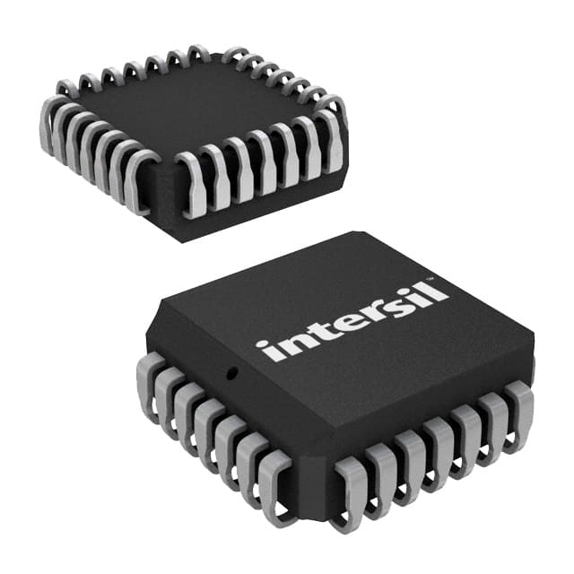
- Part No.:
- CS82C54-12Z96
- Manufacturer:
- Renesas
- Category:
- Programmable Timers and Oscillators
- Package:
- 28-LCC (J-Lead)
- Datasheet:
-
 CS82C54-12Z96.pdf
- Description:
- IC OSC PROG TIMER 12MHZ 28PLCC
- Quantity:
- Payment:

- Shipping:

Inventory:3,107
Please send an inquiry. Send us your inquiry, and we will respond immediately.
Product details
Overview
CS82C54-12Z96 from Intersil is a CMOS programmable interval timer IC with three independent 16-bit counters, supporting up to 12MHz clock input frequency, binary or BCD counting, six programmable modes, and TTL-compatible 5V operation - used for real-time clock generation, event counting, and programmable rate control in legacy x86 embedded systems.
For engineers reviewing the CS82C54-12Z96 datasheet, CS82C54-12Z96 pinout, CS82C54-12Z96 application, or CS82C54-12Z96 equivalent, this page delivers verified timing parameters, PLCC-28 package mapping, counter-mode behavior, read-back command functionality, and direct alternatives for industrial control and retro-computing designs requiring NMOS 8254 drop-in compatibility.
Technical Context
The CS82C54-12Z96 implements three fully independent 16-bit synchronous down counters, each configurable via an 8-bit control word register using A0/A1 address decoding and RD/WR strobes. Its static CMOS architecture enables low-power operation (10µA standby, 10mA at 8MHz) while maintaining full functional equivalence with the NMOS 8254.
It supports status read-back commands for latching count values and output/state flags per counter, and features dual-byte count loading with null-count flag tracking - critical for deterministic timing in interrupt-driven firmware where precise mode transitions and atomic counter reads are required.
Key Specifications
| Parameter | Value and Actual Design Meaning |
|---|---|
| Clock Input Frequency | Up to 12MHz - enables precise microsecond-scale timing intervals in high-speed 80C86/80C286 systems. |
| Counter Width | 16-bit presettable down counters - provides 65,536-step resolution for long-duration delays or high-frequency event counting. |
| Operating Voltage | +4.5V to +5.5V - ensures robust interoperability with standard TTL/CMOS logic and legacy 5V bus architectures. |
| Power Consumption | 10µA standby / 10mA active at 8MHz - reduces thermal load and simplifies power budgeting in fanless industrial controllers. |
| Temperature Range | 0°C to +70°C - qualified for commercial-grade embedded applications including PC AT clones and industrial I/O modules. |
| Package Type | 28-Lead PLCC (N28.45) - surface-mount compatible with automated assembly and reflow-solderable per RoHS Pb-free plus anneal spec. |
| Logic Compatibility | Fully TTL-compatible inputs/outputs - eliminates level-shifting requirements when interfacing with 80C88, 80C186, or discrete glue logic. |
Pinout & Package
CS82C54-12Z96 is housed in a 28-lead plastic leaded chip carrier (PLCC) package per drawing N28.45, with gull-wing leads and a 0.050" pitch. The package supports Pb-free reflow soldering and is rated for commercial temperature operation (0°C to +70°C).
| Pin/Terminal | Circuit Role | Design Meaning |
|---|---|---|
| D0–D7 | Data Bus I/O | Bi-directional 8-bit data interface tied directly to CPU data bus; three-state controlled by RD/WR/CS. |
| A0, A1 | Address Select | Selects Counter 0, 1, 2, or Control Word Register; maps to CPU A0/A1 for memory-mapped I/O access. |
| CS | Chip Select | Active-low enable; gates RD/WR operations - allows multiple timers on shared bus with decoder-based addressing. |
| RD, WR | Read/Write Strobes | Edge-triggered control signals synchronized to CPU bus cycles; qualified by CS for peripheral isolation. |
| CLK0–CLK2 | Counter Clock Inputs | Independent asynchronous clock sources per counter; accept up to 12MHz TTL-level signals. |
| GATE0–GATE2 | Counter Enable Inputs | Level-sensitive gate controls counting enable/disable; rising-edge trigger not required - supports software gating. |
| OUT0–OUT2 | Counter Output Signals | Open-drain compatible outputs reflecting current mode state (e.g., terminal count pulse or square wave). |
| VCC, GND | Power Supply | +5V supply and ground pins; decoupling capacitor (0.1µF) recommended at VCC–GND for noise immunity. |
Key Features
| Feature | Design Value |
|---|---|
| Six Programmable Counter Modes | Enables flexible use as one-shot, rate generator, square-wave oscillator, or interrupt timer - eliminating need for external logic in timing-critical firmware. |
| Status Read-Back Command | Allows atomic capture of counter output state, null-count flag, and programmed mode - essential for debugging and safe runtime reconfiguration. |
| Binary or BCD Counting | Supports both 16-bit binary (65,536 max) and decade-coded BCD (9999 max) - simplifies human-readable timekeeping and display driver integration. |
| Three Independent Counters | Permits concurrent timing tasks (e.g., system tick, watchdog timeout, PWM generation) without CPU polling or resource contention. |
| Static CMOS Architecture | Delivers zero dynamic power at idle and predictable propagation delays - critical for deterministic real-time response in safety-critical subsystems. |
Applications
| Industrial PLC Timing Module | Legacy x86 System Timer |
|---|---|
Use Scenario: Precise 10ms–1s interval generation for cyclic I/O scanning and motion control sequencing in DIN-rail mounted PLCs. IC Role / Device Role / Timing Role: Primary programmable interval timer providing deterministic interrupt triggers synchronized to ladder logic scan cycles. Use Value: Enables jitter-free 1kHz system tick with hardware reload - reducing CPU overhead by >95% versus software loops and improving cycle repeatability to ±1 CLK period. |
Use Scenario: Replacement for NMOS 8254 in IBM PC/AT-compatible motherboards and single-board computers based on 80C86/80C286 CPUs. IC Role / Device Role / Timing Role: System timer managing DRAM refresh, keyboard controller handshake, and speaker tone generation via three dedicated counters. Use Value: Direct pin-and-function compatibility with NMOS 8254 ensures zero PCB changes while cutting power consumption by 70% and extending thermal margin. |
| Embedded Watchdog & Reset Controller | Motor Speed Feedback Interface |
Use Scenario: Fail-safe timeout supervision for firmware execution in medical device controllers where missed watchdog resets must trigger hardware reset within 100ms. IC Role / Device Role / Timing Role: Dedicated counter configured in Mode 1 (programmable one-shot) to generate non-retriggerable reset pulses upon GATE deassertion. Use Value: Guarantees hard reset within 100ms ±5ns regardless of CPU lockup - meeting IEC 62304 Class C safety requirements without external components. |
Use Scenario: High-resolution RPM measurement from quadrature encoder signals in servo drives operating at 0–10,000 RPM. IC Role / Device Role / Timing Role: Event counter capturing rising edges on CLK0 while GATE0 is held high, with automatic 16-bit rollover handling via software read-back. Use Value: Achieves 0.1% speed resolution at 10,000 RPM using 1MHz base clock - eliminating FPGA or microcontroller timer resource allocation. |
Equivalent & Alternatives
The following parts are listed as comparable options for similar programmable timer applications.
| Alternative Part | Technical Difference | Application Difference | Selection Advice |
|---|---|---|---|
| CS82C54-10Z96 | 10MHz max clock frequency; otherwise identical electrical and functional specification. | Lower timing resolution in high-speed applications (e.g., >100kHz rate generation). | Select only if system clock domain is ≤10MHz and cost sensitivity outweighs performance headroom. |
| Intel 8254-10 | NMOS process; higher ICCOP (20mA), no standby current spec, wider VCC tolerance (+4.75V to +5.25V). | Not RoHS compliant; requires level-shifting for mixed-logic systems; incompatible with Pb-free reflow. | Use only for legacy repair or NMOS-only board refurbishment where CMOS leakage or thermal constraints are non-critical. |
Compared with CS82C54-12Z96, CS82C54-10Z96 trades 2MHz bandwidth for marginal cost reduction, while Intel 8254-10 sacrifices power efficiency and modern compliance for absolute NMOS pin-for-pin equivalence - making CS82C54-12Z96 the optimal choice for new designs requiring reliability, low power, and RoHS conformance.
Availability
CS82C54-12Z96 is available at Aetrix Electronics and suitable for industrial PLC timing modules, legacy x86 system timer replacements, embedded watchdog controllers, motor feedback interfaces, and retro-computing restoration projects requiring stable component supply and long-term lifecycle support.
Supply support for CS82C54-12Z96 includes scheduled delivery planning, volume procurement assistance, BOM continuity management, traceable sourcing, and lifecycle availability coordination for OEM customers, industrial embedded developers, connected-device designers, and electronics production programs.
Manufacturer
Intersil Corporation was a U.S.-based semiconductor company specializing in high-performance analog and mixed-signal ICs, later acquired by Renesas Electronics in 2017. Its legacy timing products remain widely deployed in industrial and computing infrastructure.
The 82C54 family was designed as a CMOS-enhanced successor to the Intel 8254, delivering identical functionality with lower power, higher noise immunity, and extended temperature range - targeting embedded controllers, PC-compatible systems, and real-time instrumentation.
FAQ
What is the maximum clock frequency supported by the CS82C54-12Z96?
The CS82C54-12Z96 supports a maximum clock input frequency of 12MHz across all three counters. This is confirmed in the AC Electrical Specifications table (Page 4, FN2970 Rev 6.00), where TCLK min = 80ns corresponds to 12.5MHz, with 12MHz specified as the rated operational limit. Exceeding this may cause metastability or incorrect counting behavior.
Is the CS82C54-12Z96 pin-compatible with the original Intel 8254?
Yes, the CS82C54-12Z96 is functionally and pin-compatible with the Intel 8254 in PLCC-28 package configuration. The pinout matches exactly per datasheet Figure 1 (Page 2), and all control signals (RD, WR, CS, A0/A1, D0–D7, CLK/GATE/OUT per counter) retain identical timing and electrical behavior - enabling direct replacement without layout modification.
Does the CS82C54-12Z96 support BCD counting mode?
Yes, the CS82C54-12Z96 supports Binary-Coded Decimal (BCD) counting mode via the BCD bit (D0) in the control word register. When set to '1', each counter operates as a 4-decade (0000–9999) BCD counter, enabling direct interface with decimal displays and legacy timekeeping firmware without software conversion.
What is the purpose of the "Null Count" flag in the CS82C54-12Z96 status register?
The Null Count flag (bit D6 in the status byte) indicates whether the most recently written count has been fully loaded from the Count Register (CR) into the active Counting Element (CE). It remains '1' until the transfer completes - preventing premature reads that would return stale or undefined values, especially during multi-byte count updates in Mode 0 or Mode 2.
Can the CS82C54-12Z96 operate from a 3.3V supply?
No, the CS82C54-12Z96 is specified only for +4.5V to +5.5V operation per DC Electrical Specifications (Page 3, FN2970 Rev 6.00). Applying 3.3V violates the minimum VCC requirement and will result in unreliable logic levels, failed counter initialization, or complete functional failure - a level shifter or 5V regulator is required for 3.3V-system integration.
CS82C54-12Z96 Specifications
- Product attributes
- Attribute value
- Manufacturer:
- Renesas
- Series:
- -
- Package/Case:
- 28-LCC (J-Lead)
- Packaging:
- Tape & Reel (TR)
- Product Status:
- Obsolete
- Type:
- Programmable Timer
- Count:
- -
- Frequency:
- 12MHz
- Voltage - Supply:
- 4.5V ~ 5.5V
- Current - Supply:
- 10 mA
- Operating Temperature:
- 0°C ~ 70°C
- Supplier Device Package:
- 28-PLCC (11.51x11.51)
- Mounting Type:
- Surface Mount
- Grade:
- -
- Qualification:
- -
CS82C54-12Z96 FAQ
1.How can I place an order for CS82C54-12Z96 through Aetrix?
Please submit a Request for Quotation (RFQ) for CS82C54-12Z96 on Aetrix. Our sales agent will provide a competitive quotation and guide you through the order confirmation once you accept the terms.
2.Are the price and stock information for CS82C54-12Z96 reliable?
The price and inventory of CS82C54-12Z96 are updated periodically and may fluctuate due to market conditions. Stock and pricing data are typically refreshed every 24 hours. Quotation validity for CS82C54-12Z96 is usually 5 days.
3.What payment methods are accepted for CS82C54-12Z96?
We accept Wire Transfer, PayPal, Credit Card, Western Union, MoneyGram, and Escrow for CS82C54-12Z96 transactions.
Note: Certain payment methods may incur a processing fee.
4.How is shipping managed for CS82C54-12Z96?
CS82C54-12Z96 orders can be shipped via leading logistics carriers, including DHL, UPS, FedEx, TNT, or Registered Mail.
Once your CS82C54-12Z96 order is processed, you will receive an email with the shipment details and tracking number.
Note: Tracking information may take up to 24 hours to appear. Express delivery typically takes 3–5 business days.
5.How can I obtain technical support or documentation for CS82C54-12Z96?
For technical support, including CS82C54-12Z96 datasheets, pinout diagrams, or application guidance, please contact our engineering support team. They can provide detailed documentation and assistance for your CS82C54-12Z96 requirements.
6.How does Aetrix verify that CS82C54-12Z96 is sourced from the original manufacturer or authorized distributors?
All CS82C54-12Z96 products on Aetrix are procured from qualified distributors and authorized channels. Our dedicated quality assurance team conducts strict verification, including traceability checks and, if necessary, third-party testing. This ensures that CS82C54-12Z96 meets industry standards.
7.What is the process for return or replacement of CS82C54-12Z96?
All CS82C54-12Z96 units undergo pre-shipment inspection (PSI). If there is an issue with CS82C54-12Z96, returns or replacements are accepted under the following conditions:
1.Quantity discrepancies, incorrect items, or visible external defects (such as breakage or corrosion), acknowledged by Aetrix.
2.The issue is reported within 90 days of delivery.
3.The CS82C54-12Z96 part is unused and in its original packaging.
Return procedure for CS82C54-12Z96:
1.Submit a request within 90 days.
2.Obtain a Return Material Authorization (RMA) from Aetrix.
CS82C54-12Z96 Tags

-
NE555DR
Texas Instruments
-
SA555DR
Texas Instruments
-
NA555DR
Texas Instruments
-
SE555DR
Texas Instruments

-
NE555P
Texas Instruments

-
CD4541BM96
Texas Instruments

-
CD4541BE
Texas Instruments
-
TLC555QDR
Texas Instruments
-
TLC555IDR
Texas Instruments
-
TLC555QDRQ1
Texas Instruments

-
TPL5010DDCR
Texas Instruments
-
TLC555CP
Texas Instruments
Tech Hub

TTL and CMOS logic families differ in thresholds, loading, output drive, power and timing. This engineering guide compares 74HC and 74HCT, calculates noise margins and checks 3.3 V/5 V compatibility.

A practical engineering guide to 3.3V and 5V logic compatibility, input thresholds, resistor dividers, translator ICs, MOSFET level shifting, I2C pull-ups, timing limits and power-sequencing risks.

The 74HC595 uses push-pull logic outputs, while the TPIC6B595 uses 50 V open-drain DMOS sinks for higher-power loads. This guide compares timing, current limits, 3.3 V interfacing, load wiring, thermal…

The 74HC595 converts serial data into eight stable parallel outputs. This guide covers pin functions, shift and storage timing, OE and MR behavior, drive-current limits, cascading, voltage compatibilit…

A technical comparison of level-sensitive latches and edge-triggered flip-flops, covering timing windows, setup and hold limits, master–slave operation, time borrowing, race-through, HDL inference and…

A D latch stores one bit while Enable controls when data can pass. This reference covers gate-level operation, truth tables, transparency, setup and hold timing, LE versus OE, common ICs and practical …

An SR latch stores one bit through cross-coupled feedback. This engineering reference covers NOR and NAND implementations, truth tables, forbidden-state recovery, gated operation, switch debouncing, fa…

Latch circuits retain one bit through feedback. This technical reference covers SR and D latches, truth tables, transparency, timing limits, latch-versus-flip-flop behavior, applications and common log…

An engineering guide to LED driver operation, constant-current and constant-voltage outputs, linear and switching topologies, dimming, IC selection, calculations, replacement compatibility, and fault c…

Operational amplifier guide covering op amp basics, feedback, ideal vs real op amps, common configurations, buffer circuits, offset, bias current, gain-bandwidth, slew rate, rail-to-rail limits and sel…


