
 My Inquiry
 My Account


Infineon Technologies CY14B256L-SZ45XI
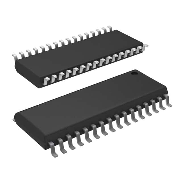
- Part No.:
- CY14B256L-SZ45XI
- Manufacturer:
- Infineon Technologies
- Category:
- Memory
- Package:
- 32-SOIC (0.295", 7.50mm Width)
- Datasheet:
-
 CY14B256L-SZ45XI.pdf
- Description:
- IC NVSRAM 256KBIT PAR 32SOIC
- Quantity:
- Payment:

- Shipping:

Inventory:2,162
Please send an inquiry. Send us your inquiry, and we will respond immediately.
Product details
Overview
CY14B256L-SZ45XI from Cypress Semiconductor is a 256 Kbit (32K × 8) nonvolatile SRAM with QuantumTrap™ technology, functioning as a drop-in SRAM replacement with integrated nonvolatile storage. It delivers 45 ns access time, operates from single 3V ±10% supply, supports AutoStore™ on power loss using external VCAP capacitor, and provides unlimited SRAM read/write cycles with 200,000 STORE endurance. Used in industrial control modules requiring persistent data retention across uncontrolled power cycles.
For engineers reviewing the CY14B256L-SZ45XI datasheet, CY14B256L-SZ45XI pinout, CY14B256L-SZ45XI application, or CY14B256L-SZ45XI equivalent, key selection criteria include AutoStore timing behavior, HSB-controlled hardware store latency, VCAP sizing for 45 ns operation, and software STORE/RECALL address sequence compliance.
Technical Context
The CY14B256L-SZ45XI integrates a standard fast SRAM array (512 × 512) with parallel QuantumTrap nonvolatile cells per bit. STORE and RECALL operations execute atomically across all 32,768 bytes, blocking concurrent SRAM access during transfer.
AutoStore triggers when VCC falls below VSWITCH (2.7 V min), using charge stored on VCAP to complete one full STORE cycle. Hardware STORE is initiated via active-low HSB with tDELAY (100 ns min) allowing pending writes to finish before nonvolatile commit.
Key Specifications
| Parameter | Value and Actual Design Meaning |
|---|---|
| Memory Density | 256 Kbit (32K × 8) - supports byte-wide interface with full 15-bit addressing (A0–A14) |
| Access Time | 45 ns - defines maximum clock-to-data valid delay for CE/OE-controlled reads at 3.6 V, 25°C |
| Supply Voltage | 3.0 V to 3.6 V - single rail operation with –10%/+20% tolerance; no 5 V support |
| STORE Endurance | 200,000 cycles - specifies maximum number of SRAM→QuantumTrap transfers before wear-out |
| Data Retention | 20 years at 55°C - guaranteed nonvolatile data hold time under industrial temperature stress |
| VCAP Requirement | 4.7 µF tantalum or ceramic - minimum capacitance on VCAP pin to sustain 45 ns STORE under worst-case VCC droop |
| Operating Temperature | –40°C to +85°C - validated performance range for industrial-grade deployment |
Pinout & Package
Package: 32-pin SOIC (300 mil width), RoHS-compliant, surface-mountable with standard JEDEC MS-012AC footprint.
| Pin/Terminal | Circuit Role | Design Meaning |
|---|---|---|
| A0–A14 | Address Input | 15-bit address bus selecting one of 32,768 memory locations; latched on CE/WE transitions |
| DQ0–DQ7 | Bidirectional Data I/O | 8-bit data path shared for read output and write input; tri-stated when OE HIGH or during STORE/RECALL |
| CE | Chip Enable | Active-low chip select; must be LOW for any SRAM access; controls CE-timed READ/WRITE cycles |
| WE | Write Enable | Active-low write strobe; LOW with CE LOW initiates write; pulled HIGH externally during power-up to prevent spurious writes |
| OE | Output Enable | Active-low output enable; controls data bus drivers during READ; must be HIGH during WRITE to avoid contention |
| HSB | Hardware Store Busy | Open-drain status/output pin: driven LOW during STORE/RECALL; pulled LOW externally to request hardware STORE |
| VCAP | AutoStore Capacitor | Charge reservoir node; internal charge pump drives it to ~5 V; supplies energy for STORE when VCC collapses |
| VCC | Power Supply | 3.0–3.6 V main supply; powers SRAM logic and QuantumTrap control circuitry |
| VSS | Ground | Reference return path for all digital and analog functions; requires low-inductance connection to system ground plane |
Key Features
| Feature | Design Value |
|---|---|
| AutoStore on Power Loss | Enables automatic, hands-off data preservation without host intervention when VCC drops below 2.7 V |
| Software STORE/RECALL | 6-step CE-controlled READ sequence (e.g., 0x0E38 → 0x0FC0) initiates nonvolatile commit or restore without hardware signal |
| Hardware STORE Control | HSB pin allows deterministic, externally timed STORE initiation with 100 ns delay to complete pending writes |
| Unlimited SRAM Cycles | Standard SRAM interface behavior preserved: no wear-out mechanism for reads/writes during normal operation |
| Data Protection Logic | Blocks WRITE and STORE during brown-out (VCC < VSWITCH) and inhibits spurious writes at power-up until CE/WE toggle |
Applications
| Industrial PLC Data Logging | Medical Device Parameter Storage |
|---|---|
Use Scenario: Persistent storage of runtime configuration and sensor calibration data in programmable logic controllers with unpredictable mains power. IC Role / Device Role / Timing Role: Nonvolatile SRAM serving as primary working memory and fail-safe backup storage; replaces battery-backed SRAM. Use Value: Eliminates battery maintenance and leakage risk while guaranteeing 20-year data retention at 55°C ambient. | Use Scenario: Storing patient-specific therapy settings and device self-test results in portable infusion pumps and diagnostic monitors. IC Role / Device Role / Timing Role: Dual-role memory: volatile workspace during operation, nonvolatile archive upon shutdown or fault detection. Use Value: Ensures regulatory-compliant data persistence across 200,000 power cycles without recalibration or manual backup. |
| Telecom Base Station Configuration | Automotive ADAS Sensor Calibration |
Use Scenario: Holding FPGA configuration checksums, RF tuning tables, and network identity keys in remote radio units subject to frequent grid interruptions. IC Role / Device Role / Timing Role: High-reliability nvSRAM interfacing directly with microcontroller's memory-mapped bus; accessed via standard SRAM protocol. Use Value: Provides 45 ns access for real-time control loops while securing critical firmware metadata against sudden power loss. | Use Scenario: Saving camera/lidar alignment offsets and thermal drift compensation coefficients in autonomous driving ECUs during vehicle ignition cycles. IC Role / Device Role / Timing Role: Nonvolatile scratchpad memory mapped into MCU address space; updated only after verified sensor characterization. Use Value: Maintains functional safety integrity (ISO 26262 ASIL-B) by ensuring calibration persistence across 100% of cold starts and brown-outs. |
Equivalent & Alternatives
The following parts are listed as comparable options for similar nonvolatile SRAM applications.
| Alternative Part | Technical Difference | Application Difference | Selection Advice |
|---|---|---|---|
| STK14D88-45I | Pin-compatible but lacks AutoStore; requires external battery or capacitor-based backup circuit | No built-in power-loss detection or VCAP-driven STORE; higher BOM cost and board area for backup components | Select when legacy STK14D88 footprint reuse is mandatory and external backup design is already validated |
| FM24V02-G | F-RAM-based; 10¹⁴ read/write endurance; no STORE/RECALL latency; 3.3 V only; 256 Kbit density | Eliminates STORE timing constraints and VCAP dependency; lower average power; no wear leveling required | Select when deterministic sub-100 ns nonvolatile writes and zero-latency recall are required over quantum-based retention |
Compared with STK14D88-45I and FM24V02-G, CY14B256L-SZ45XI uniquely combines SRAM-speed interface, integrated AutoStore with VCAP simplicity, and 20-year retention-making it optimal where battery-free reliability and legacy SRAM compatibility are jointly essential.
Availability
CY14B256L-SZ45XI is available at Aetrix Electronics and suitable for industrial PLCs, medical infusion devices, telecom base stations, and automotive ADAS ECUs requiring stable component supply with long-term lifecycle assurance.
Supply support for CY14B256L-SZ45XI includes scheduled delivery planning, volume procurement assistance, BOM continuity management, traceable sourcing, and lifecycle availability coordination for OEM customers, industrial embedded developers, connected-device designers, and electronics production programs.
Manufacturer
Cypress Semiconductor (now part of Infineon Technologies) designs high-performance mixed-signal ICs for embedded systems, focusing on memory, PSoC, USB, and timing solutions.
The CY14B nvSRAM product line targets applications needing seamless SRAM functionality with guaranteed nonvolatile data retention-designed specifically to replace battery-backed SRAM in industrial, medical, and communications equipment.
FAQ
What is the minimum VCAP capacitance required for reliable AutoStore operation at 45 ns?
The CY14B256L-SZ45XI requires a minimum 4.7 µF tantalum or low-ESR ceramic capacitor on the VCAP pin to ensure successful STORE completion during VCC collapse. This value is derived from the 45 ns access time specification and internal charge pump characteristics, and must be placed within 10 mm of the VCAP pin with short, wide traces to minimize inductance.
Can the HSB pin be left unconnected if hardware STORE is not used?
Yes. The HSB pin has an internal weak pull-up resistor and may be left floating if hardware STORE initiation is not required. However, if the system monitors HSB for STORE status, it must be externally pulled up to VCC with a 10 kΩ resistor and routed with controlled impedance to avoid noise-induced false triggers during high-speed operation.
How does the CY14B256L-SZ45XI prevent data corruption during brown-out conditions?
The device incorporates voltage monitoring that disables all externally initiated STORE and WRITE operations when VCC falls below VSWITCH (2.7 V). It also inhibits writes at power-up until a negative edge is detected on CE or WE, preventing spurious writes during unstable supply ramp-up-ensuring data integrity without host firmware intervention.
Is the software STORE sequence compatible with all microcontroller bus interfaces?
Yes-the six-address READ sequence (0x0E38, 0x31C7, 0x03E0, 0x3C1F, 0x303F, 0x0FC0) uses standard CE-controlled or OE-controlled reads and requires no special timing beyond tAA. It works with any 8-bit parallel bus controller capable of precise address sequencing, including ARM Cortex-M, Renesas RX, and legacy 8051 derivatives.
CY14B256L-SZ45XI Specifications
- Product attributes
- Attribute value
- Manufacturer:
- Infineon Technologies
- Series:
- -
- Package/Case:
- 32-SOIC (0.295", 7.50mm Width)
- Packaging:
- Tube
- Product Status:
- Obsolete
- Programmable:
- Not Verified
- Memory Type:
- Non-Volatile
- Memory Format:
- NVSRAM
- Technology:
- NVSRAM (Non-Volatile SRAM)
- Memory Size:
- 256Kbit
- Memory Organization:
- 32K x 8
- Memory Interface:
- Parallel
- Clock Frequency:
- -
- Write Cycle Time - Word, Page:
- 45ns
- Access Time:
- 45 ns
- Voltage - Supply:
- 2.7V ~ 3.6V
- Operating Temperature:
- -40°C ~ 85°C (TA)
- Grade:
- -
- Qualification:
- -
- Mounting Type:
- Surface Mount
- Supplier Device Package:
- 32-SOIC
CY14B256L-SZ45XI FAQ
1.How can I place an order for CY14B256L-SZ45XI through Aetrix?
Please submit a Request for Quotation (RFQ) for CY14B256L-SZ45XI on Aetrix. Our sales agent will provide a competitive quotation and guide you through the order confirmation once you accept the terms.
2.Are the price and stock information for CY14B256L-SZ45XI reliable?
The price and inventory of CY14B256L-SZ45XI are updated periodically and may fluctuate due to market conditions. Stock and pricing data are typically refreshed every 24 hours. Quotation validity for CY14B256L-SZ45XI is usually 5 days.
3.What payment methods are accepted for CY14B256L-SZ45XI?
We accept Wire Transfer, PayPal, Credit Card, Western Union, MoneyGram, and Escrow for CY14B256L-SZ45XI transactions.
Note: Certain payment methods may incur a processing fee.
4.How is shipping managed for CY14B256L-SZ45XI?
CY14B256L-SZ45XI orders can be shipped via leading logistics carriers, including DHL, UPS, FedEx, TNT, or Registered Mail.
Once your CY14B256L-SZ45XI order is processed, you will receive an email with the shipment details and tracking number.
Note: Tracking information may take up to 24 hours to appear. Express delivery typically takes 3–5 business days.
5.How can I obtain technical support or documentation for CY14B256L-SZ45XI?
For technical support, including CY14B256L-SZ45XI datasheets, pinout diagrams, or application guidance, please contact our engineering support team. They can provide detailed documentation and assistance for your CY14B256L-SZ45XI requirements.
6.How does Aetrix verify that CY14B256L-SZ45XI is sourced from the original manufacturer or authorized distributors?
All CY14B256L-SZ45XI products on Aetrix are procured from qualified distributors and authorized channels. Our dedicated quality assurance team conducts strict verification, including traceability checks and, if necessary, third-party testing. This ensures that CY14B256L-SZ45XI meets industry standards.
7.What is the process for return or replacement of CY14B256L-SZ45XI?
All CY14B256L-SZ45XI units undergo pre-shipment inspection (PSI). If there is an issue with CY14B256L-SZ45XI, returns or replacements are accepted under the following conditions:
1.Quantity discrepancies, incorrect items, or visible external defects (such as breakage or corrosion), acknowledged by Aetrix.
2.The issue is reported within 90 days of delivery.
3.The CY14B256L-SZ45XI part is unused and in its original packaging.
Return procedure for CY14B256L-SZ45XI:
1.Submit a request within 90 days.
2.Obtain a Return Material Authorization (RMA) from Aetrix.
CY14B256L-SZ45XI Tags

-
M24C02-WMN6TP
STMicroelectronics

-
AT24C02C-XHM-T
Microchip Technology

-
AT21CS01-STUM10-T
Microchip Technology

-
AT24C02C-SSHM-T
Microchip Technology

-
24LC01BT-I/OT
Microchip Technology

-
M24C02-FMC6TG
STMicroelectronics
-
AT24CS02-SSHM-T
Microchip Technology

-
93LC46BT-I/OT
Microchip Technology
-
AT24C04C-SSHM-T
Microchip Technology

-
24LC01BT-I/SN
Microchip Technology
-
24AA02UIDT-I/OT
Microchip Technology

-
AT24C08C-STUM-T
Microchip Technology
Tech Hub
A technical comparison of level-sensitive latches and edge-triggered flip-flops, covering timing windows, setup and hold limits, master–slave operation, time borrowing, race-through, HDL inference and…
A D latch stores one bit while Enable controls when data can pass. This reference covers gate-level operation, truth tables, transparency, setup and hold timing, LE versus OE, common ICs and practical …

An SR latch stores one bit through cross-coupled feedback. This engineering reference covers NOR and NAND implementations, truth tables, forbidden-state recovery, gated operation, switch debouncing, fa…

Latch circuits retain one bit through feedback. This technical reference covers SR and D latches, truth tables, transparency, timing limits, latch-versus-flip-flop behavior, applications and common log…

An engineering guide to LED driver operation, constant-current and constant-voltage outputs, linear and switching topologies, dimming, IC selection, calculations, replacement compatibility, and fault c…

Operational amplifier guide covering op amp basics, feedback, ideal vs real op amps, common configurations, buffer circuits, offset, bias current, gain-bandwidth, slew rate, rail-to-rail limits and sel…

Jumper cables guide covering safe connection order, red and black clamp placement, final ground connection, cable gauge, length, clamp quality, copper vs CCA cables, jump starter comparison and battery…

LDO regulator guide covering low dropout voltage, power dissipation, thermal design, PSRR, output noise, capacitor stability, adjustable LDO circuits, LDO vs buck converter and datasheet selection chec…

Conditional Access Module guide covering CAM meaning, CI/CI+ interface, smart card authorization, DVB security workflow, TV and set-top box compatibility, internal electronics, ESD protection, connecto…

Guide to electronic component obsolescence covering EOL risk, PCN/PDN notices, last-time buy planning, replacement options, form-fit-function validation, counterfeit risk and BOM lifecycle management.


