
 My Inquiry
 My Account


Infineon Technologies CY25701FLXIT
- Part No.:
- CY25701FLXIT
- Manufacturer:
- Infineon Technologies
- Category:
- Programmable Timers and Oscillators
- Package:
- 4-CLCC
- Datasheet:
-
 CY25701FLXIT.pdf
- Description:
- IC OSC XTAL PROG 4-CLCC
- Quantity:
- Payment:

- Shipping:

Inventory:2,200
Please send an inquiry. Send us your inquiry, and we will respond immediately.
Product details
Overview
CY25701FLXIT from Cypress Semiconductor is a programmable high-frequency crystal oscillator with selectable spread spectrum (SSXO) or no-spread (XO) operation, delivering 10–166 MHz output clock signals with ±0.25% to ±2.0% center spread or –0.5% to –4.0% down spread, 3.3 V supply, and industrial temperature range (–40 °C to +85 °C), used for EMI reduction in PC motherboard clock trees.
For engineers reviewing the CY25701FLXIT datasheet, CY25701FLXIT pinout, CY25701FLXIT application, or CY25701FLXIT equivalent, key selection criteria include programmable spread percentage, 85 ps cycle-to-cycle jitter at 133 MHz, OE-controlled output enable/disable timing, 4-pin ceramic LCC package compatibility, and factory/field programming flexibility via CY3672-USB kit.
Technical Context
The CY25701FLXIT integrates a proprietary PLL to synthesize output frequencies from an embedded crystal, supporting both SSXO and XO modes via nonvolatile configuration memory. Spread modulation is fixed at 31.5 kHz nominal (30.1–32.9 kHz selectable), with programmable spread percentages mapped to discrete codes (e.g., Code A = ±0.25%, Code G = –0.5%).
It operates exclusively from a 3.3 V supply (3.0–3.6 V range), delivers CMOS-compatible output drive (12 mA source/sink), and features asynchronous OE control with 150–350 ns enable/disable delays. Output duty cycle is tightly controlled (45–55%) and load capacitance is specified up to 15 pF.
Key Specifications
| Parameter | Value and Actual Design Meaning |
|---|---|
| Output Frequency Range | 10–166 MHz; covers PCIe Gen1–Gen3 reference clocks, USB 2.0/3.0 PHY clocks, and DDR memory interface timing. |
| Spread Spectrum Modulation | 31.5 kHz nominal; reduces peak EMI amplitude by spreading energy across narrowband harmonics, easing FCC/CE compliance. |
| Center Spread Range | ±0.25% to ±2.0%; enables fine-tuned EMI suppression without violating system timing margins. |
| Cycle-to-Cycle Jitter | 85 ps typical at 133 MHz; ensures stable setup/hold timing for high-speed SerDes and memory controllers. |
| Operating Temperature | –40 °C to +85 °C; qualified for industrial-grade embedded systems including network switches and industrial PCs. |
| Supply Voltage | 3.3 V ±10%; compatible with standard logic rail without level-shifting or regulation overhead. |
| Output Enable Delay | 150–350 ns; supports synchronized power-up sequencing in multi-rail SoC platforms. |
Pinout & Package
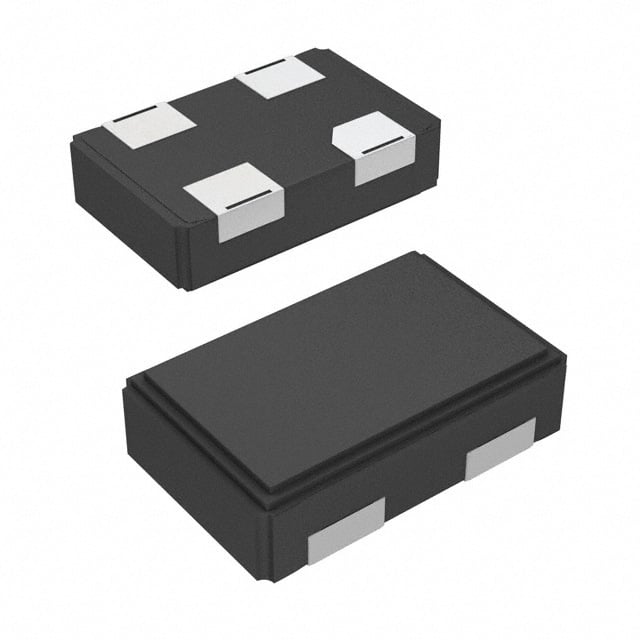
Package: 4-pin ceramic leadless chip carrier (LCC), surface-mount, Pb-free, 5.0 × 3.2 mm footprint, industrial-grade thermal performance.
| Pin/Terminal | Circuit Role | Design Meaning |
|---|---|---|
| 1 (OE) | Output Enable input | CMOS-compatible active-HIGH control; places SSCLK output in high-impedance state when low, enabling clock gating in power-managed systems. |
| 2 (VSS) | Ground reference | Dedicated analog/digital ground return path; must be connected to low-impedance PCB ground plane to minimize jitter and EMI. |
| 3 (SSCLK) | Modulated clock output | CMOS-level output (12 mA drive) carrying either spread-spectrum or fixed-frequency clock signal; requires ≤15 pF capacitive load. |
| 4 (VDD) | Power supply input | 3.3 V supply pin; requires local 0.1 µF decoupling capacitor placed within 2 mm of pin to suppress supply noise-induced jitter. |
Key Features
| Feature | Design Value |
|---|---|
| Field-programmable configuration memory | Enables post-manufacture customization of output frequency and spread percentage without mask changes or NRE fees. |
| Asynchronous OE control | Allows dynamic clock shutdown during idle states without PLL relock delay, reducing system standby power. |
| Integrated PLL with embedded crystal | Eliminates external crystal and loop filter components, reducing BOM count and board area in space-constrained designs. |
| Industrial temperature qualification | Validated operation across –40 °C to +85 °C ensures reliability in uncontrolled ambient environments like factory automation controllers. |
| Pb-free ceramic LCC package | Meets RoHS and JEDEC MSL-3 requirements; compatible with standard reflow profiles and automated SMT assembly. |
Applications
| PC Motherboard Clock Tree | Network Switch Timing |
|---|---|
Use Scenario: Provides primary reference clock for CPU, PCIe, SATA, and USB controllers on x86-based motherboards. IC Role / Device Role / Timing Role: System-level clock source with spread spectrum enabled to meet FCC Class B radiated emissions limits. Use Value: Reduces need for costly metal shielding and ferrite beads while maintaining timing integrity across multiple high-speed interfaces. | Use Scenario: Supplies synchronized 125 MHz clock to Ethernet PHYs and packet processors in Layer 2/L3 switches. IC Role / Device Role / Timing Role: Low-jitter, programmable clock generator supporting both IEEE 1588 PTP synchronization and deterministic latency paths. Use Value: Enables single-part clocking for mixed-rate PHYs (1G/2.5G/10G) with configurable spread to pass CISPR 22 conducted emission tests. |
| Industrial PLC Controller | Consumer Set-Top Box |
Use Scenario: Generates 66 MHz system clock for ARM Cortex-A9-based controller running real-time Linux and fieldbus stacks. IC Role / Device Role / Timing Role: Industrial-grade oscillator with guaranteed operation at –40 °C, supporting cold-start reliability in outdoor enclosures. Use Value: Eliminates external temperature-compensated crystal oscillator (TCXO), lowering cost and improving long-term aging stability (±5 ppm/year). | Use Scenario: Drives HDMI transmitter, video decoder, and audio DAC in HD digital cable receivers. IC Role / Device Role / Timing Role: Dual-mode clock source-XO mode for audio sample rate accuracy, SSXO mode for video subsystem EMI reduction. Use Value: Allows one component to serve both precision timing and regulatory compliance needs, simplifying BOM and layout validation. |
Equivalent & Alternatives
The following parts are listed as comparable options for similar programmable oscillator applications.
| Alternative Part | Technical Difference | Application Difference | Selection Advice |
|---|---|---|---|
| Si5351A-B-GM | Multi-output I²C-programmable clock generator; no integrated crystal; higher jitter (150 ps) at 133 MHz. | Requires external crystal and I²C host control; suited for multi-clock domain systems, not single-output replacement. | Select only if multiple independent outputs or frequency agility beyond 166 MHz are required. |
| ICS843001AGI-01LFT | Fixed-frequency LVDS oscillator; no spread spectrum; ±50 ppm stability; 3.3 V; 4-pin LCC. | Lacks programmability and EMI reduction capability; limited to non-regulated or shielded environments. | Choose only for cost-sensitive, non-EMI-critical applications where fixed 100 MHz or 125 MHz is sufficient. |
Compared with Si5351A-B-GM and ICS843001AGI-01LFT, CY25701FLXIT uniquely combines embedded crystal, field-programmable spread control, and industrial temperature rating in a single-output 4-pin LCC-making it optimal for EMI-constrained, single-rail embedded clocking where simplicity and qualification assurance are critical.
Availability
CY25701FLXIT is available at Aetrix Electronics and suitable for PC motherboard design, industrial PLC timing, and network switch clocking requiring stable component supply, long-lifecycle availability, and consistent parametric performance across production batches.
Supply support for CY25701FLXIT includes scheduled delivery planning, volume procurement assistance, BOM continuity management, traceable sourcing, and lifecycle availability coordination for OEM customers, industrial embedded developers, connected-device designers, and electronics production programs.
Manufacturer
Cypress Semiconductor (now part of Infineon Technologies) designs high-performance timing, memory, and programmable logic solutions for embedded systems, with global R&D and manufacturing infrastructure.
The CY25701 product line targets EMI-sensitive digital systems requiring certified, programmable clock sources-emphasizing ease of integration, regulatory compliance acceleration, and field configurability without hardware redesign.
FAQ
What is the default spread spectrum setting for CY25701FLXIT?
The device ships unprogrammed; no default spread is preloaded. Factory or field programming is required to set spread percentage (e.g., ±0.5%, –2.0%) or select XO mode (±0.0%). Programming uses CY3672-USB kit and CyberClocks™ software, with configuration stored in on-chip nonvolatile memory.
Can CY25701FLXIT operate at 2.5 V?
No. CY25701FLXIT is specified only for 3.3 V operation (3.0–3.6 V range). Operation below 3.0 V violates absolute maximum ratings and may cause PLL unlock, output instability, or permanent configuration corruption. A dedicated 3.3 V LDO or regulator rail is mandatory.
Is the SSCLK output edge-aligned or phase-aligned across spread modulation cycles?
The SSCLK output maintains consistent phase alignment relative to the internal PLL reference; modulation introduces controlled frequency deviation but preserves edge monotonicity and duty cycle stability (45–55%). No phase discontinuities or glitches occur during spread transitions-verified per AC Electrical Characteristics Table on page 5.
Does CY25701FLXIT require external passive components for basic operation?
Only a 0.1 µF ceramic decoupling capacitor between VDD and VSS is required. No external crystal, loop filter, or termination resistors are needed-the oscillator is fully self-contained. Layout best practice mandates placing the capacitor within 2 mm of pins 2 and 4 to maintain jitter performance.
CY25701FLXIT Specifications
- Product attributes
- Attribute value
- Manufacturer:
- Infineon Technologies
- Series:
- -
- Package/Case:
- 4-CLCC
- Packaging:
- Tape & Reel (TR)
- Product Status:
- Obsolete
- Type:
- Oscillator, Crystal
- Count:
- -
- Frequency:
- 10MHz ~ 166MHz
- Voltage - Supply:
- 3V ~ 3.6V
- Current - Supply:
- 50 mA
- Operating Temperature:
- -40°C ~ 85°C
- Supplier Device Package:
- 4-CLCC (5x3.2)
- Mounting Type:
- Surface Mount
- Grade:
- -
- Qualification:
- -
CY25701FLXIT FAQ
1.How can I place an order for CY25701FLXIT through Aetrix?
Please submit a Request for Quotation (RFQ) for CY25701FLXIT on Aetrix. Our sales agent will provide a competitive quotation and guide you through the order confirmation once you accept the terms.
2.Are the price and stock information for CY25701FLXIT reliable?
The price and inventory of CY25701FLXIT are updated periodically and may fluctuate due to market conditions. Stock and pricing data are typically refreshed every 24 hours. Quotation validity for CY25701FLXIT is usually 5 days.
3.What payment methods are accepted for CY25701FLXIT?
We accept Wire Transfer, PayPal, Credit Card, Western Union, MoneyGram, and Escrow for CY25701FLXIT transactions.
Note: Certain payment methods may incur a processing fee.
4.How is shipping managed for CY25701FLXIT?
CY25701FLXIT orders can be shipped via leading logistics carriers, including DHL, UPS, FedEx, TNT, or Registered Mail.
Once your CY25701FLXIT order is processed, you will receive an email with the shipment details and tracking number.
Note: Tracking information may take up to 24 hours to appear. Express delivery typically takes 3–5 business days.
5.How can I obtain technical support or documentation for CY25701FLXIT?
For technical support, including CY25701FLXIT datasheets, pinout diagrams, or application guidance, please contact our engineering support team. They can provide detailed documentation and assistance for your CY25701FLXIT requirements.
6.How does Aetrix verify that CY25701FLXIT is sourced from the original manufacturer or authorized distributors?
All CY25701FLXIT products on Aetrix are procured from qualified distributors and authorized channels. Our dedicated quality assurance team conducts strict verification, including traceability checks and, if necessary, third-party testing. This ensures that CY25701FLXIT meets industry standards.
7.What is the process for return or replacement of CY25701FLXIT?
All CY25701FLXIT units undergo pre-shipment inspection (PSI). If there is an issue with CY25701FLXIT, returns or replacements are accepted under the following conditions:
1.Quantity discrepancies, incorrect items, or visible external defects (such as breakage or corrosion), acknowledged by Aetrix.
2.The issue is reported within 90 days of delivery.
3.The CY25701FLXIT part is unused and in its original packaging.
Return procedure for CY25701FLXIT:
1.Submit a request within 90 days.
2.Obtain a Return Material Authorization (RMA) from Aetrix.
CY25701FLXIT Tags

-
NE555DR
Texas Instruments
-
SA555DR
Texas Instruments
-
NA555DR
Texas Instruments
-
SE555DR
Texas Instruments

-
NE555P
Texas Instruments

-
CD4541BM96
Texas Instruments

-
CD4541BE
Texas Instruments
-
TLC555QDR
Texas Instruments
-
TLC555IDR
Texas Instruments
-
TLC555QDRQ1
Texas Instruments

-
TPL5010DDCR
Texas Instruments
-
TLC555CP
Texas Instruments
Tech Hub

Operational amplifier guide covering op amp basics, feedback, ideal vs real op amps, common configurations, buffer circuits, offset, bias current, gain-bandwidth, slew rate, rail-to-rail limits and sel…

Jumper cables guide covering safe connection order, red and black clamp placement, final ground connection, cable gauge, length, clamp quality, copper vs CCA cables, jump starter comparison and battery…

LDO regulator guide covering low dropout voltage, power dissipation, thermal design, PSRR, output noise, capacitor stability, adjustable LDO circuits, LDO vs buck converter and datasheet selection chec…

Conditional Access Module guide covering CAM meaning, CI/CI+ interface, smart card authorization, DVB security workflow, TV and set-top box compatibility, internal electronics, ESD protection, connecto…

Guide to electronic component obsolescence covering EOL risk, PCN/PDN notices, last-time buy planning, replacement options, form-fit-function validation, counterfeit risk and BOM lifecycle management.

18650 battery guide covering lithium-ion cell basics, 3.6V/3.7V voltage, 4.2V charging, mAh and Wh capacity, protected cells, chargers, BMS, series-parallel packs, holders, welding and sourcing checks.…

Hall effect sensor guide covering working principle, linear and digital sensors, Arduino circuits, current sensing, speed detection, automotive applications, A3144 examples, signal filtering and datash…

Product Change Notification guide for electronic components, covering PCN meaning, PCN vs PDN/EOL, common change types, risk levels, form-fit-function review, engineering validation, BOM control, LTB/L…

A practical guide to blend door actuators, covering HVAC function, symptoms, location, AC and heater issues, reset and calibration, replacement cost, electrical diagnosis, compatibility checks, and rep…

Engineering guide to Raspberry Pi alternatives, covering chip-level differences, Orange Pi, ROCK, Jetson, Banana Pi, NanoPi, Compute Module, Pico, GPIO, camera, HAT compatibility, and replacement risks…


