
 My Inquiry
 My Account


Infineon Technologies CY28329OXC
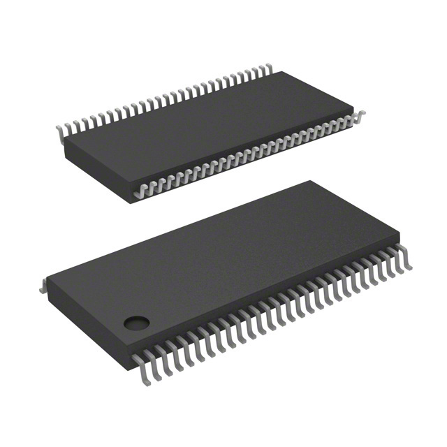
- Part No.:
- CY28329OXC
- Manufacturer:
- Infineon Technologies
- Package:
- 56-BSSOP (0.295", 7.50mm Width)
- Datasheet:
-
 CY28329OXC.pdf
- Description:
- IC CLOCK DRIVER 56SSOP
- Quantity:
- Payment:

- Shipping:

Inventory:3,699
Please send an inquiry. Send us your inquiry, and we will respond immediately.
Product details
Overview
CY28329OXC from Cypress Semiconductor is a 133-MHz spread-spectrum clock synthesizer/driver with four pairs of differential CPU outputs, ten synchronous PCI clocks, six 3.3V 66-MHz clocks, two fixed 48-MHz USB/DOT clocks, and one 14.318-MHz reference output - all in a single 56-pin SSOP package. It integrates dual PLLs, SMBus programmability, and power-down control (PD#, PCI_STOP#) for motherboard-level timing in multi-CPU, AGP, and PCI/ISA systems.
For engineers reviewing the CY28329OXC datasheet, CY28329OXC pinout, CY28329OXC application, or CY28329OXC equivalent, this device supports ACPI-compliant power management, EMI reduction via down-spread spectrum, configurable CPU frequency selection (100/133 MHz), and per-output enable/disable via SMBus - critical for high-density PC motherboard and chipset clocking design.
Technical Context
The CY28329OXC employs two independent PLLs: PLL1 generates CPU and REF clocks from a 14.318-MHz crystal input, while PLL2 derives PCI, 3V66, and USB clocks from either the 66-MHz internal VCO or external 66IN. Its SMBus interface (slave address 0xD2) enables runtime configuration of 32 registers for individual buffer enable/disable, VCH/66MHz mode selection, and spread-spectrum activation.
It supports three-level mode select (S2) and dual LVTTL inputs (S1, MULT0) to configure CPU frequency and output current drive strength (via IREF resistor). VTTPWRGD# strobes input sampling at power-up, ensuring deterministic initialization of S1/S2/MULT0 before clock distribution begins.
Key Specifications
| Parameter | Value and Actual Design Meaning |
|---|---|
| Max CPU Output Frequency | 133 MHz - supports Pentium III/IV-class dual-processor motherboards with differential signaling compliance. |
| Spread Spectrum Range | Down-spread only, ±0.25% - reduces EMI peak amplitude without requiring system-level redesign. |
| Output Types | Four differential CPU pairs (Type X1, 50 Ω), ten PCI (Type 5), six 3V66, two 48-MHz USB/DOT (Type 3A/3B), one REF - each with independent enable control. |
| Supply Voltage | 3.135–3.465 V - compatible with standard 3.3V logic rails; no sequencing required between VDD_CORE, VDD_CPU, and VDD_PCI. |
| Jitter Performance | CPU cycle-cycle jitter ≤150 ps - meets Intel's CPU clock stability requirement for 133-MHz FSB operation. |
| SMBus Address | 0xD2 (11010010) - supports block write only; enables post-power-up reconfiguration of all clock buffers and modes. |
| Power-Down Current | 25–45 mA (depending on IREF setting) - achieves >90% current reduction vs. active mode (360 mA) during ACPI S3/S4 states. |
Pinout & Package
Package: 56-pin SSOP (0.209" body width), RoHS-compliant, JEDEC MO-153 compliant. Thermal pad not present; standard PCB land pattern applies.
| Pin/Terminal | Circuit Role | Design Meaning |
|---|---|---|
| REF (Pin 56) | Reference Clock Output | 3.3V CMOS 14.318-MHz output; drives chipset PLL reference input with <1 ns skew tolerance. |
| CPU0–CPU3 / CPU0#–CPU3# (Pins 44,45,48,49,51,52,53,54) | Differential CPU Clock Outputs | Four LVDS-compatible pairs; each pair delivers matched rise/fall times (175–700 ps) and <150 ps inter-pair skew. |
| PCI0–PCI6 (Pins 10,11,12,13,16,17,18) | Synchronous PCI Clock Outputs | Seven 33-MHz outputs derived from 66IN or internal 66-MHz VCO; individually controllable via SMBus register Byte 2. |
| 3V66_0 (Pin 33), 3V66_1/VCH (Pin 35) | 66-MHz / 48-MHz Selectable Outputs | 3V66_0 fixed at 66 MHz; 3V66_1/VCH configurable via SMBus Bit 5 to output either 66 MHz or 48 MHz for USB host controller sync. |
| USB (Pin 39), DOT (Pin 38) | Fixed 48-MHz Clock Outputs | Guaranteed +167 ppm accuracy for USB 1.1 compliance; edge-rate programmable via SMBus Byte 5 Bits 1 & 3. |
| PD# (Pin 25), PCI_STOP# (Pin 34) | Active-Low Power Control Inputs | Hardware-driven shutdown: PD# disables all outputs except REF; PCI_STOP# halts PCI[0:6] while preserving PCI_F[0:2] free-running mode. |
Key Features
| Feature | Design Value |
|---|---|
| Dual PLL Architecture | Independent PLL1 (CPU/REF) and PLL2 (PCI/3V66/USB) prevent cross-domain jitter coupling and allow asynchronous frequency domains. |
| Per-Output SMBus Enable/Disable | 32-byte register map allows runtime masking of any clock buffer - essential for dynamic power gating in ACPI S0ix states. |
| VCH/66MHz Mode Switching | SMBus Bit 5 toggles Pin 35 between 66 MHz (AGP hub link) and 48 MHz (USB host) - eliminates need for external multiplexer. |
| VTTPWRGD# Strobed Initialization | Ensures S1/S2/MULT0 inputs are sampled only after VTT rail stabilization - guarantees deterministic boot-time CPU frequency selection. |
| Configurable Output Drive Strength | IREF resistor (221 Ω or 475 Ω) sets CPU output current (4× or 6× IREF), enabling optimization for trace impedance (50 Ω) and stub length. |
Applications
| Desktop Motherboard Clocking | Multi-CPU Server Board |
|---|---|
|
Use Scenario: ATX motherboard supporting dual Pentium 4 processors, AGP 4x graphics, and six PCI slots. IC Role / Device Role / Timing Role: Primary clock synthesizer generating synchronized CPU, PCI, AGP, and USB clocks from single crystal. Use Value: Eliminates need for discrete clock buffers and multiple oscillators; reduces BOM count by 7+ components while meeting Intel's 133-MHz FSB skew spec (<150 ps). |
Use Scenario: Dual-Xeon server board with hot-plug PCI slots and integrated USB 1.1 host controller. IC Role / Device Role / Timing Role: Central timing hub providing isolated 133-MHz CPU clocks, 33-MHz PCI clocks, and 48-MHz USB clocks with independent enable control. Use Value: SMBus register Byte 3 enables per-slot PCI clock gating during hot-plug events, reducing insertion transients and meeting PICMG R2.0 slot power sequencing requirements. |
| ACPI-Compliant Power Management | EMI-Sensitive Industrial PC |
|
Use Scenario: Embedded industrial PC entering S3 suspend-to-RAM state with CPU and memory clocks halted. IC Role / Device Role / Timing Role: Hardware-controlled power-down via PD# signal disables all clocks except REF, minimizing standby current to 25 mA. Use Value: Meets ACPI 2.0 "G3 Mechanical Off" current budget; REF remains active to support RTC and wake-event detection circuitry. |
Use Scenario: Fanless medical imaging PC operating in enclosed metal chassis with strict FCC Class B radiated emissions limits. IC Role / Device Role / Timing Role: Spread-spectrum clocking (0.25% down-spread) applied to CPU and PCI outputs to lower 100–200 MHz harmonic peaks. Use Value: Reduces 133-MHz fundamental harmonics by 8–10 dBµV/m at 3 m, enabling pass on first EMC test without ferrite beads or shielding modifications. |
Equivalent & Alternatives
Cypress CY28329OXC has two functionally aligned alternatives with documented compatibility in motherboard reference designs.
| Alternative Part | Technical Difference | Application Difference | Selection Advice |
|---|---|---|---|
| IDT 87010AGLFT | Single PLL architecture; no SMBus interface; fixed 133/100 MHz CPU outputs; no VCH/48-MHz mode switching. | Lacks runtime configurability - requires hardware strap changes for USB vs. AGP mode; no per-output enable. | Select when cost-sensitive, low-feature-count designs prioritize pin-for-pin replacement over flexibility. |
| ICS 952002AF | Supports 166-MHz CPU outputs; includes integrated 2.5V VTT regulator; SMBus read capability; no spread-spectrum. | Enables next-gen Pentium 4 FSB upgrades but increases thermal load; requires additional decoupling for VTT rail. | Select when future-proofing for 166-MHz platforms is required and EMI reduction is handled externally. |
Compared with IDT 87010AGLFT and ICS 952002AF, CY28329OXC uniquely balances SMBus configurability, spread-spectrum EMI suppression, and dual-PLL isolation - making it optimal for mid-life-cycle motherboard revisions requiring both USB 1.1 timing and legacy PCI/ISA support without hardware respins.
Availability
CY28329OXC is available at Aetrix Electronics and suitable for desktop motherboard manufacturing, multi-CPU server board production, and industrial PC OEM programs requiring stable component supply and long-term lifecycle support.
Supply support for CY28329OXC includes scheduled delivery planning, volume procurement assistance, BOM continuity management, traceable sourcing, and lifecycle availability coordination for OEM customers, industrial embedded developers, connected-device designers, and electronics production programs.
Manufacturer
Cypress Semiconductor (now part of Infineon Technologies) is a fabless semiconductor company specializing in timing, memory, and programmable logic solutions for computing and communications infrastructure.
The CY28xxx series was designed specifically for x86-based PC motherboard clock generation - integrating spread-spectrum, multi-domain PLLs, and SMBus control to replace discrete clock trees in cost- and space-constrained designs.
FAQ
What is the function of VTTPWRGD# on CY28329OXC?
VTTPWRGD# is a level-sensitive strobe that signals when the VTT voltage rail has stabilized. The device samples S1, S2, and MULT0 inputs only after VTTPWRGD# goes LOW, ensuring deterministic CPU frequency and drive strength selection at power-up. Once sampled, further transitions on VTTPWRGD# are ignored.
Can CY28329OXC generate both 48 MHz and 66 MHz simultaneously?
Yes. Pin 35 (3V66_1/VCH) is configurable via SMBus register Byte 0 Bit 5 to output either 66 MHz (AGP hub link) or 48 MHz (USB host), while Pins 38 (DOT) and 39 (USB) deliver fixed 48-MHz clocks, and Pin 33 (3V66_0) provides fixed 66-MHz - enabling concurrent 48/66-MHz timing domains without external logic.
How does spread-spectrum clocking work on CY28329OXC?
CY28329OXC implements down-spread spectrum only, modulating the CPU and PCI output frequencies by ±0.25% around their nominal values using a triangular waveform. This spreads energy across a 25–35 kHz bandwidth, lowering peak radiated emissions by up to 10 dBµV/m - verified per FCC Part 15 and CISPR 22 standards.
Is the 56-pin SSOP package of CY28329OXC pin-compatible with TSSOP?
Yes. The CY28329OXC is offered in both 56-pin SSOP (CY28329OXC) and 56-pin TSSOP (CY28329AXC) variants with identical pinout, electrical characteristics, and thermal specifications. Footprint compatibility allows direct substitution in existing layouts without PCB revision.
CY28329OXC Specifications
- Product attributes
- Attribute value
- Manufacturer:
- Infineon Technologies
- Series:
- -
- Package/Case:
- 56-BSSOP (0.295", 7.50mm Width)
- Packaging:
- Tube
- Product Status:
- Obsolete
- Programmable:
- Not Verified
- Type:
- Clock Driver, Clock/Frequency Synthesizer, Fanout Distribution, Spread Spectrum Clock Generator
- PLL:
- Yes
- Input:
- LVTTL, Crystal
- Output:
- Clock
- Number of Circuits:
- 1
- Ratio - Input:Output:
- 1:22
- Differential - Input:Output:
- No/Yes
- Frequency - Max:
- 133MHz
- Divider/Multiplier:
- Yes/No
- Voltage - Supply:
- 3.135V ~ 3.465V
- Operating Temperature:
- 0°C ~ 70°C
- Mounting Type:
- Surface Mount
- Grade:
- -
- Qualification:
- -
- Supplier Device Package:
- 56-SSOP
CY28329OXC FAQ
1.How can I place an order for CY28329OXC through Aetrix?
Please submit a Request for Quotation (RFQ) for CY28329OXC on Aetrix. Our sales agent will provide a competitive quotation and guide you through the order confirmation once you accept the terms.
2.Are the price and stock information for CY28329OXC reliable?
The price and inventory of CY28329OXC are updated periodically and may fluctuate due to market conditions. Stock and pricing data are typically refreshed every 24 hours. Quotation validity for CY28329OXC is usually 5 days.
3.What payment methods are accepted for CY28329OXC?
We accept Wire Transfer, PayPal, Credit Card, Western Union, MoneyGram, and Escrow for CY28329OXC transactions.
Note: Certain payment methods may incur a processing fee.
4.How is shipping managed for CY28329OXC?
CY28329OXC orders can be shipped via leading logistics carriers, including DHL, UPS, FedEx, TNT, or Registered Mail.
Once your CY28329OXC order is processed, you will receive an email with the shipment details and tracking number.
Note: Tracking information may take up to 24 hours to appear. Express delivery typically takes 3–5 business days.
5.How can I obtain technical support or documentation for CY28329OXC?
For technical support, including CY28329OXC datasheets, pinout diagrams, or application guidance, please contact our engineering support team. They can provide detailed documentation and assistance for your CY28329OXC requirements.
6.How does Aetrix verify that CY28329OXC is sourced from the original manufacturer or authorized distributors?
All CY28329OXC products on Aetrix are procured from qualified distributors and authorized channels. Our dedicated quality assurance team conducts strict verification, including traceability checks and, if necessary, third-party testing. This ensures that CY28329OXC meets industry standards.
7.What is the process for return or replacement of CY28329OXC?
All CY28329OXC units undergo pre-shipment inspection (PSI). If there is an issue with CY28329OXC, returns or replacements are accepted under the following conditions:
1.Quantity discrepancies, incorrect items, or visible external defects (such as breakage or corrosion), acknowledged by Aetrix.
2.The issue is reported within 90 days of delivery.
3.The CY28329OXC part is unused and in its original packaging.
Return procedure for CY28329OXC:
1.Submit a request within 90 days.
2.Obtain a Return Material Authorization (RMA) from Aetrix.
CY28329OXC Tags

-
CD74HCT4046AM96
Texas Instruments

-
MC14046BDWR2G
onsemi

-
501MILFT
Renesas Electronics Corporation
-
CD74HC7046AM
Texas Instruments

-
CDCVF2505PWR
Texas Instruments

-
RC19004A100GNL#KB0
Renesas Electronics Corporation

-
SI5351A-B-GTR
Skyworks Solutions Inc.

-
CY2305SXI-1T
Infineon Technologies
-
570BILFT
Renesas Electronics Corporation

-
CDCE913PWR
Texas Instruments
-
CY2305SXI-1HT
Infineon Technologies

-
DS1086LU+T
Analog Devices Inc./Maxim Integrated
Tech Hub

An engineering guide to LED driver operation, constant-current and constant-voltage outputs, linear and switching topologies, dimming, IC selection, calculations, replacement compatibility, and fault c…

Operational amplifier guide covering op amp basics, feedback, ideal vs real op amps, common configurations, buffer circuits, offset, bias current, gain-bandwidth, slew rate, rail-to-rail limits and sel…

Jumper cables guide covering safe connection order, red and black clamp placement, final ground connection, cable gauge, length, clamp quality, copper vs CCA cables, jump starter comparison and battery…

LDO regulator guide covering low dropout voltage, power dissipation, thermal design, PSRR, output noise, capacitor stability, adjustable LDO circuits, LDO vs buck converter and datasheet selection chec…

Conditional Access Module guide covering CAM meaning, CI/CI+ interface, smart card authorization, DVB security workflow, TV and set-top box compatibility, internal electronics, ESD protection, connecto…

Guide to electronic component obsolescence covering EOL risk, PCN/PDN notices, last-time buy planning, replacement options, form-fit-function validation, counterfeit risk and BOM lifecycle management.

18650 battery guide covering lithium-ion cell basics, 3.6V/3.7V voltage, 4.2V charging, mAh and Wh capacity, protected cells, chargers, BMS, series-parallel packs, holders, welding and sourcing checks.…

Hall effect sensor guide covering working principle, linear and digital sensors, Arduino circuits, current sensing, speed detection, automotive applications, A3144 examples, signal filtering and datash…

Product Change Notification guide for electronic components, covering PCN meaning, PCN vs PDN/EOL, common change types, risk levels, form-fit-function review, engineering validation, BOM control, LTB/L…

A practical guide to blend door actuators, covering HVAC function, symptoms, location, AC and heater issues, reset and calibration, replacement cost, electrical diagnosis, compatibility checks, and rep…


