
 My Inquiry
 My Account


Infineon Technologies CY37064P100-125AC
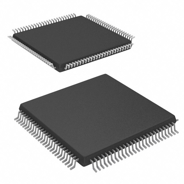
- Part No.:
- CY37064P100-125AC
- Manufacturer:
- Infineon Technologies
- Package:
- 100-LQFP
- Datasheet:
-
 CY37064P100-125AC.pdf
- Description:
- IC CPLD 64MC 10NS 100TQFP
- Quantity:
- Payment:

- Shipping:

Inventory:3,167
Please send an inquiry. Send us your inquiry, and we will respond immediately.
Product details
Overview
CY37064P100-125AC from Cypress Semiconductor is a 64-macrocell In-System Reprogrammable (ISR™) Complex Programmable Logic Device (CPLD) in the Ultra37000 family, operating at 5V with 100-pin TQFP package and 125 MHz maximum frequency (tPD = 12.5 ns). It features four synchronous clocks, programmable bus-hold on all I/Os, and JTAG-compliant ISR for field reconfiguration without pinout or timing changes. Used in legacy PCI interface logic, system boot configuration, and FPGA companion control.
For engineers reviewing the CY37064P100-125AC datasheet, CY37064P100-125AC pinout, CY37064P100-125AC application, or CY37064P100-125AC equivalent, key selection criteria include macrocell count, I/O pin count (69), tPD timing bin (125), VCCO voltage flexibility (5V/3.3V I/O support), and JTAG boundary-scan compliance for testability.
Technical Context
The CY37064P100-125AC implements a modular architecture with two logic blocks, each containing 32 macrocells, a 72×87 product term array, and an intelligent product term allocator supporting 0–16 product terms per macrocell. All inputs route through a fully global Programmable Interconnect Matrix (PIM) with no fanout, expander, or PIM-induced delay penalties.
It supports flexible clocking via four dedicated synchronous clocks (CLK0–CLK3) and one asynchronous product term clock (PTCLK), with polarity control per logic block. Bus-hold and slew-rate control are programmable per I/O, and all I/Os are 5V-tolerant when VCCO = 3.3V - critical for mixed-voltage board interfacing.
Key Specifications
| Parameter | Value and Actual Design Meaning |
|---|---|
| Macrocells | 64 total, distributed across two logic blocks - enables medium-complexity glue logic without FPGA overhead. |
| Maximum Frequency (fMAX) | 125 MHz - guarantees deterministic timing for PCI Local Bus and control-plane logic up to 33 MHz system clocks. |
| Propagation Delay (tPD) | 12.5 ns - fixed worst-case path delay, independent of fanout or product term sharing due to PIM architecture. |
| I/O Pins | 69 user-programmable I/Os in 100-pin TQFP - supports dense peripheral bridging with fixed pinout across speed bins. |
| VCCO Support | Configurable 5V or 3.3V output levels - allows direct interfacing to both TTL and JEDEC-compliant CMOS buses without level shifters. |
| JTAG Interface | IEEE 1149.1-compliant - enables in-system reprogramming, boundary-scan testing, and design iteration without hardware modification. |
| Power Supply (VCC) | 5.0V ± 5% - requires single 5V rail; VCCO pins independently set for I/O voltage level selection. |
Pinout & Package
Packaged in a 100-lead Thin Quad Flat Package (TQFP), the CY37064P100-125AC uses a standard 0.5 mm pitch, 14 × 14 mm body size, with exposed thermal pad (non-electrical) and lead-free finish compliant with RoHS Directive 2011/65/EU.
| Pin/Terminal | Circuit Role | Design Meaning |
|---|---|---|
| TCK, TMS, TDI, TDO | JTAG Test Access Port | Enable boundary-scan testing and serial ISP programming; TDO is open-drain, others are CMOS-compatible inputs. |
| CLK0–CLK3 | Dedicated Clock Inputs | Four globally distributed synchronous clocks; each configurable for rising/falling edge triggering per logic block. |
| OE[0:3] | Output Enable Controls | Four programmable OE product terms - each controls up to eight macrocells, enabling fine-grained tri-state management. |
| VCCO[0:3] | I/O Power Supply | Four independent VCCO pins - grouped to supply specific I/O banks; setting to 3.3V enables 5V-tolerant outputs. |
| GND, VCC | Power Distribution | 12 GND and 4 VCC pins - ensure low-noise power delivery and reduce simultaneous switching noise in high-speed logic. |
Key Features
| Feature | Design Value |
|---|---|
| In-System Reprogrammability (ISR™) | JTAG-based field updates preserve pinout and timing - eliminates PCB respins during firmware-driven logic revisions. |
| Programmable Bus-Hold | Weak latch on every I/O - maintains last valid state during high-Z, eliminating external pull-ups in bus-hold applications like address/data latching. |
| Flexible Product Term Allocation | 0–16 product terms assignable per macrocell - supports heterogeneous logic depth (e.g., wide decoders + narrow state machines) in same device. |
| Programmable Slew Rate | Fast/slow edge selection per output - reduces EMI in noise-sensitive environments while retaining full-speed capability where needed. |
| Dedicated Input/Clock Pins | Five dedicated inputs including four clock-capable pins - simplifies clock domain crossing and eliminates routing congestion for timing-critical paths. |
Applications
| PCI Bus Interface Logic | Legacy System Boot Configuration |
|---|---|
Use Scenario: Translating between 32-bit PCI Local Bus signals and custom ASIC control registers in industrial controllers. IC Role / Device Role / Timing Role: Glue logic CPLD handling address decoding, burst termination, and parity generation with deterministic 12.5 ns tPD. Use Value: Eliminates need for discrete logic or FPGA in cost-sensitive, low-volume embedded systems requiring PCI compliance and field-upgradable firmware. |
Use Scenario: Storing and sequencing boot-time configuration bits for microcontrollers and FPGAs during power-on reset. IC Role / Device Role / Timing Role: Nonvolatile configuration manager using buried macrocells as static registers and I/O macrocells as parallel output latches. Use Value: Provides deterministic, JTAG-reprogrammable boot logic independent of flash memory wear-out or corruption risks. |
| FPGA Companion Control | Industrial I/O Expansion |
Use Scenario: Managing configuration, reset, and status handshaking between host processor and Xilinx Spartan FPGA in motor drive systems. IC Role / Device Role / Timing Role: Synchronous control hub synchronizing multi-cycle FPGA configuration with processor-initiated commands via CLK0–CLK3. Use Value: Enables safe, glitch-free FPGA reconfiguration without external sequencers - leveraging ISR to update handshake protocols post-deployment. |
Use Scenario: Expanding GPIO count and implementing debounce, edge detection, and interrupt prioritization for PLC I/O modules. IC Role / Device Role / Timing Role: Real-time digital signal conditioner with programmable bus-hold on input pins and slew-controlled outputs driving optocouplers. Use Value: Reduces BOM count by replacing multiple discrete buffers, RC networks, and Schmitt triggers with single reconfigurable logic block. |
Equivalent & Alternatives
The following parts are listed as comparable options for similar CPLD-based glue logic applications.
| Alternative Part | Technical Difference | Application Difference | Selection Advice |
|---|---|---|---|
| XC9572XL-10VQG44C | 72 macrocells, 44-pin VQFP, 3.3V-only supply, 10 ns tPD - lacks VCCO flexibility and 5V tolerance. | Requires level-shifting for 5V legacy buses; unsuitable for mixed-voltage PCI designs without external translators. | Select only if system operates exclusively at 3.3V and board space constraints favor smaller package. |
| ATF1504AS-10AU100 | 128 macrocells, 100-pin TQFP, 3.3V supply, 10 ns tPD - higher density but no 5V operation or VCCO-selectable I/O. | Cannot replace CY37064P100-125AC in 5V systems without redesign; JTAG implementation differs in boundary-scan register mapping. | Prefer for new 3.3V-only designs needing >64 macrocells and faster timing, but verify JTAG toolchain compatibility. |
Compared with XC9572XL-10VQG44C and ATF1504AS-10AU100, the CY37064P100-125AC uniquely supports dual-voltage I/O via VCCO pins and retains full 5V system compatibility - making it irreplaceable in legacy PCI and mixed-rail industrial backplanes where voltage translation adds cost and failure modes.
Availability
CY37064P100-125AC is available at Aetrix Electronics and suitable for PCI interface logic, FPGA companion control, and industrial I/O expansion requiring stable component supply across long-lifecycle embedded programs.
Supply support for CY37064P100-125AC includes scheduled delivery planning, volume procurement assistance, BOM continuity management, traceable sourcing, and lifecycle availability coordination for OEM customers, industrial embedded developers, connected-device designers, and electronics production programs.
Manufacturer
Cypress Semiconductor (now part of Infineon Technologies) is a U.S.-based semiconductor company specializing in programmable logic, memory, and mixed-signal solutions for industrial, automotive, and communications markets.
The Ultra37000 CPLD family was designed to deliver high-density, pin-compatible, and timing-predictable logic replacement for 22V10-style devices - targeting cost-sensitive, long-lifecycle applications where reprogrammability and mixed-voltage interoperability are essential.
FAQ
Is CY37064P100-125AC compatible with 3.3V I/O signaling?
Yes. The device supports 3.3V I/O levels when VCCO pins are connected to 3.3V; all I/Os remain 5V-tolerant in this mode, meeting JEDEC 3.3V CMOS specifications. This allows seamless interfacing with both 3.3V and 5V peripherals without external level shifters.
Does CY37064P100-125AC require external configuration memory?
No. It is electrically erasable and nonvolatile - configuration data is stored internally in EEPROM cells. After power-up, the device operates immediately without relying on external PROM or flash memory, reducing BOM count and boot latency.
Can the JTAG interface be used for both programming and debugging?
Yes. The IEEE 1149.1-compliant JTAG port supports boundary-scan testing (BST), in-system reprogramming (ISP), and real-time visibility into internal logic states during emulation - enabling hardware validation and field firmware updates without physical access to configuration pins.
What is the maximum number of product terms usable per macrocell?
Up to 16 product terms can be allocated to any single macrocell via the intelligent product term allocator. This allocation is dynamic and software-determined during place-and-route - no hardware limitation prevents full utilization of all 80 local product terms across the 32-macrocell logic block.
CY37064P100-125AC Specifications
- Product attributes
- Attribute value
- Manufacturer:
- Infineon Technologies
- Series:
- Ultra37000™
- Package/Case:
- 100-LQFP
- Packaging:
- Bag
- Product Status:
- Obsolete
- Programmable:
- Not Verified
- Programmable Type:
- In-System Reprogrammable™ (ISR™) CMOS
- Delay Time tpd(1) Max:
- 10 ns
- Voltage Supply - Internal:
- 4.75V ~ 5.25V
- Number of Logic Elements/Blocks:
- -
- Number of Macrocells:
- 64
- Number of Gates:
- -
- Number of I/O:
- 69
- Operating Temperature:
- 0°C ~ 70°C (TA)
- Grade:
- -
- Qualification:
- -
- Mounting Type:
- Surface Mount
- Supplier Device Package:
- 100-TQFP (14x14)
CY37064P100-125AC FAQ
1.How can I place an order for CY37064P100-125AC through Aetrix?
Please submit a Request for Quotation (RFQ) for CY37064P100-125AC on Aetrix. Our sales agent will provide a competitive quotation and guide you through the order confirmation once you accept the terms.
2.Are the price and stock information for CY37064P100-125AC reliable?
The price and inventory of CY37064P100-125AC are updated periodically and may fluctuate due to market conditions. Stock and pricing data are typically refreshed every 24 hours. Quotation validity for CY37064P100-125AC is usually 5 days.
3.What payment methods are accepted for CY37064P100-125AC?
We accept Wire Transfer, PayPal, Credit Card, Western Union, MoneyGram, and Escrow for CY37064P100-125AC transactions.
Note: Certain payment methods may incur a processing fee.
4.How is shipping managed for CY37064P100-125AC?
CY37064P100-125AC orders can be shipped via leading logistics carriers, including DHL, UPS, FedEx, TNT, or Registered Mail.
Once your CY37064P100-125AC order is processed, you will receive an email with the shipment details and tracking number.
Note: Tracking information may take up to 24 hours to appear. Express delivery typically takes 3–5 business days.
5.How can I obtain technical support or documentation for CY37064P100-125AC?
For technical support, including CY37064P100-125AC datasheets, pinout diagrams, or application guidance, please contact our engineering support team. They can provide detailed documentation and assistance for your CY37064P100-125AC requirements.
6.How does Aetrix verify that CY37064P100-125AC is sourced from the original manufacturer or authorized distributors?
All CY37064P100-125AC products on Aetrix are procured from qualified distributors and authorized channels. Our dedicated quality assurance team conducts strict verification, including traceability checks and, if necessary, third-party testing. This ensures that CY37064P100-125AC meets industry standards.
7.What is the process for return or replacement of CY37064P100-125AC?
All CY37064P100-125AC units undergo pre-shipment inspection (PSI). If there is an issue with CY37064P100-125AC, returns or replacements are accepted under the following conditions:
1.Quantity discrepancies, incorrect items, or visible external defects (such as breakage or corrosion), acknowledged by Aetrix.
2.The issue is reported within 90 days of delivery.
3.The CY37064P100-125AC part is unused and in its original packaging.
Return procedure for CY37064P100-125AC:
1.Submit a request within 90 days.
2.Obtain a Return Material Authorization (RMA) from Aetrix.
CY37064P100-125AC Tags
-
5M40ZE64C5N
Intel
-
ATF1502ASV-15AU44
Microchip Technology
-
5M80ZE64C5N
Intel
-
5M80ZT100C5N
Intel
-
ATF1502AS-10AU44
Microchip Technology
-
ATF1502AS-10JU44
Microchip Technology
-
5M80ZE64I5N
Intel
-
5M80ZT100I5N
Intel
-
LC4032V-75TN48C
Lattice Semiconductor Corporation
-
ATF1504ASV-15AU44
Microchip Technology
-
ATF1504AS-10JU44
Microchip Technology
-
5M160ZE64C5N
Intel
Tech Hub

An engineering guide to LED driver operation, constant-current and constant-voltage outputs, linear and switching topologies, dimming, IC selection, calculations, replacement compatibility, and fault c…

Operational amplifier guide covering op amp basics, feedback, ideal vs real op amps, common configurations, buffer circuits, offset, bias current, gain-bandwidth, slew rate, rail-to-rail limits and sel…

Jumper cables guide covering safe connection order, red and black clamp placement, final ground connection, cable gauge, length, clamp quality, copper vs CCA cables, jump starter comparison and battery…

LDO regulator guide covering low dropout voltage, power dissipation, thermal design, PSRR, output noise, capacitor stability, adjustable LDO circuits, LDO vs buck converter and datasheet selection chec…

Conditional Access Module guide covering CAM meaning, CI/CI+ interface, smart card authorization, DVB security workflow, TV and set-top box compatibility, internal electronics, ESD protection, connecto…

Guide to electronic component obsolescence covering EOL risk, PCN/PDN notices, last-time buy planning, replacement options, form-fit-function validation, counterfeit risk and BOM lifecycle management.

18650 battery guide covering lithium-ion cell basics, 3.6V/3.7V voltage, 4.2V charging, mAh and Wh capacity, protected cells, chargers, BMS, series-parallel packs, holders, welding and sourcing checks.…

Hall effect sensor guide covering working principle, linear and digital sensors, Arduino circuits, current sensing, speed detection, automotive applications, A3144 examples, signal filtering and datash…

Product Change Notification guide for electronic components, covering PCN meaning, PCN vs PDN/EOL, common change types, risk levels, form-fit-function review, engineering validation, BOM control, LTB/L…

A practical guide to blend door actuators, covering HVAC function, symptoms, location, AC and heater issues, reset and calibration, replacement cost, electrical diagnosis, compatibility checks, and rep…


