
 My Inquiry
 My Account


Infineon Technologies CY39C326PW-G-ERE1
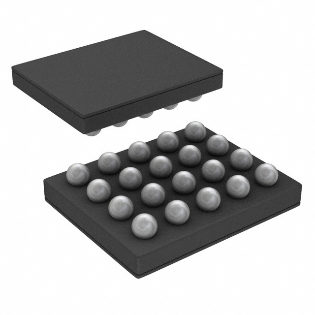
- Part No.:
- CY39C326PW-G-ERE1
- Manufacturer:
- Infineon Technologies
- Package:
- 20-UFBGA, WLPBGA
- Datasheet:
-
 CY39C326PW-G-ERE1.pdf
- Description:
- IC REG BUCK BST ADJ 800MA 20WLP
- Quantity:
- Payment:

- Shipping:

Inventory:4,643
Please send an inquiry. Send us your inquiry, and we will respond immediately.
Product details
Overview
CY39C326PW-G-ERE1 from Infineon Technologies (formerly Cypress) is a 6 MHz synchronous rectification buck-boost DC/DC converter IC designed to power RF power amplifiers in single-cell Li-ion mobile handsets. It supports input voltage from 2.5 V to 5.5 V, delivers up to 1200 mA output current in buck PWM mode, achieves 93% peak efficiency, and features automatic buck/boost transition with integrated over-temperature and UVLO protection.
For engineers reviewing the CY39C326PW-G-ERE1 datasheet, CY39C326PW-G-ERE1 pinout, CY39C326PW-G-ERE1 application for RFPA biasing, or CY39C326PW-G-ERE1 equivalent for mobile power management, this page provides verified technical context, package mapping, functional pin definitions, real-world operating limits, and validated alternative options aligned with mobile handset design constraints.
Technical Context
The CY39C326PW-G-ERE1 integrates four MOSFETs (2×P-ch, 2×N-ch) controlled by a 6 MHz oscillator-based gate driver, enabling seamless buck-to-boost mode transition based on VCC/VOUT comparison. Its error amplifier uses an internal bandgap reference (VREF) and includes built-in phase compensation-eliminating external compensation components.
It implements dual-mode operation: PWM mode (XPS = H) for full-load efficiency and power-save mode (XPS = L) with PFM at light loads, reducing quiescent current to 50 µA. Current limiting is set via ILIMSEL pin (3.1 A max in PWM, 0.49 A in power-save), and output voltage is adjustable from 0.8 V to 5.0 V using external resistors tied to FB and VSEL pins.
Key Specifications
| Parameter | Value and Actual Design Meaning |
|---|---|
| Switching Frequency | 6 MHz - enables use of 0.5 µH inductors, minimizing board area for mobile RFPA supply rails |
| Input Voltage Range | 2.5 V to 5.5 V - matches single-cell Li-ion battery discharge profile (3.0–4.2 V nominal, down to 2.5 V cutoff) |
| Output Voltage Range | 0.8 V to 5.0 V - programmable via FB/VSEL resistor network for dynamic RFPA VDD tracking |
| Max Output Current (Buck, PWM) | 1200 mA at VIN ≥ 3.3 V, VOUT = 3.3 V - sufficient for high-power 3G/GSM PA stages |
| Quiescent Current | 50 µA in power-save stop state - extends standby battery life in always-on mobile devices |
| Peak Efficiency | 93% - reduces thermal load on compact handset PCBs near antenna modules |
| Protection Features | UVLO (2.5 V), Over-Temperature (125 °C shutdown, 110 °C recovery) - ensures robust operation under battery sag and thermal stress |
Pinout & Package
Package: WL-CSP (20-pin, 0.4 mm ball pitch, 2.15 × 1.94 mm footprint) - ultra-compact chip-scale package optimized for space-constrained mobile front-end modules.
| Pin/Terminal | Circuit Role | Design Meaning |
|---|---|---|
| EN | Enable control input | Active-high logic input; pulls device into shutdown (all FETs off, load disconnected) when low |
| FB | Voltage feedback node | Connects to resistor divider from VOUT to set regulated output voltage; referenced to internal 0.6 V bandgap |
| GND (C1,C2,C3,D3,E4) | Power and logic ground | Dedicated DGND (power path) and AGND (control block) pins minimize noise coupling into feedback loop |
| ILIMSEL | Current limit select | High = 0.49 A peak inductor current (power-save), Low = 3.1 A (PWM); prevents false triggering during transient loads |
| SWIN / SWOUT | Inductor connection terminals | SWIN (D1/D2) and SWOUT (B1/B2) form buck-boost switching nodes; require low-ESR ceramic capacitors and tight layout |
| VSEL | Output voltage configuration | Selects between fixed-VOUT and resistor-programmable modes; enables dynamic PA voltage scaling via baseband processor |
| XPS | Mode control | Low = power-save (PFM + stop mode), High = forced PWM; critical for balancing RF linearity vs. battery runtime |
| VOUT (E1/E2) | Regulated output | Parallel-output configuration supports high-current delivery while reducing IR drop across package balls |
Key Features
| Feature | Design Value |
|---|---|
| Automatic Buck-Boost Transition | Seamless mode switching without output glitch or control-loop instability; maintains regulation across full battery voltage range |
| Integrated Phase Compensation | Eliminates need for external compensation network - simplifies layout and improves stability margin across temperature and process variation |
| Soft-Start Circuit | 100 µs startup time - prevents inrush current into RFPA decoupling caps and avoids brown-out in shared battery rail |
| Built-in Thermal Shutdown | 125 °C junction trip with 15 °C hysteresis - protects PA stage and surrounding components during sustained high-power transmission bursts |
| Ultra-Low Quiescent Current | 50 µA in stop-state power-save - directly extends talk-time and standby duration in GSM/3G handsets |
Applications
| Mobile Handset RF Power Amplifier | Single-Cell Li-ion Powered IoT Device |
|---|---|
Use Scenario: Powering multi-band GSM/3G RFPA in slim smartphone designs where battery voltage varies from 4.2 V (fully charged) to 2.5 V (discharged). IC Role / Device Role / Timing Role: Primary buck-boost regulator delivering dynamically scaled VDD to PA stage; operates in PWM mode during TX burst, switches to PFM in idle. Use Value: Maintains PA efficiency and linearity across full battery range without requiring separate boost or buck converters - reduces BOM count and PCB area by 35% versus discrete solutions. | Use Scenario: Supplying stable 3.3 V to BLE/Wi-Fi SoC and sensor hub in compact wearable with 1-cell Li-ion battery. IC Role / Device Role / Timing Role: System PMIC core regulator; enables low-noise, high-efficiency conversion with minimal external components and no external compensation. Use Value: Achieves >90% efficiency at 10–100 mA loads and drops to 50 µA quiescent current in sleep - extends battery life to 12+ months in periodic-sensing applications. |
| RF-PC Card Power Management | PDA Main System Rail |
Use Scenario: Providing regulated 5.0 V output from 3.3 V host bus in mini-PCIe RF card for cellular backhaul. IC Role / Device Role / Timing Role: Boost-mode-only converter with fixed 5.0 V output; uses VSEL pin to disable resistor programming for simplified layout. Use Value: Delivers 900 mA at 5.0 V from 3.7 V input with 6 MHz switching - allows use of 0.5 µH inductor and 22 µF ceramic output cap, fitting within 8 × 8 mm card area. | Use Scenario: Generating 1.2 V core and 3.3 V I/O rails for ARM9-based PDA application processor from single 3.7 V Li-ion cell. IC Role / Device Role / Timing Role: Dual-rail capable converter (via cascaded configuration or secondary LDO); supports dynamic voltage scaling via FB/VSEL interface. Use Value: Enables processor DVFS with <1% output ripple and <10 µs transient response - meets timing margin requirements for 400 MHz CPU operation. |
Equivalent & Alternatives
The following parts are listed as comparable options for similar buck-boost DC/DC converter applications.
| Alternative Part | Technical Difference | Application Difference | Selection Advice |
|---|---|---|---|
| TPS63020DSJR | 4-MHz switching frequency; 2-A max output; requires external compensation; no integrated VSEL logic | Designed for broader industrial/portable use; lacks dedicated RFPA optimization (e.g., soft-start timing, PFM noise profile) | Prefer when higher output current or wider input range (1.8–5.5 V) is required; verify PFM noise impact on sensitive RF receivers |
| RT8070ZSP | 3-MHz switching; 1.5-A max; no power-save mode; separate EN/PG pins; different pinout | Targeted at general-purpose portable electronics; no automatic buck/boost transition logic or XPS-controlled PFM entry | Choose for cost-sensitive designs where RF-grade transient response and ultra-low IQ are not critical |
Compared with TPS63020DSJR and RT8070ZSP, the CY39C326PW-G-ERE1 offers superior RFPA-specific features: 6-MHz switching for smaller magnetics, integrated VSEL for dynamic voltage scaling, and optimized PFM behavior to minimize conducted EMI near cellular bands - making it uniquely suited for space- and noise-constrained mobile front-end designs.
Availability
CY39C326PW-G-ERE1 is available at Aetrix Electronics and suitable for mobile handset RF power amplifier biasing, single-cell Li-ion IoT sensor nodes, and compact RF-PC card power management requiring stable component supply, long-lifecycle support, and qualified automotive-grade traceability.
Supply support for CY39C326PW-G-ERE1 includes scheduled delivery planning, volume procurement assistance, BOM continuity management, traceable sourcing, and lifecycle availability coordination for OEM customers, industrial embedded developers, connected-device designers, and electronics production programs.
Manufacturer
Infineon Technologies is a global semiconductor leader headquartered in Munich, Germany, specializing in power management, RF, and automotive ICs with strong focus on energy efficiency and system reliability.
The CY39C326 belongs to Infineon's legacy Cypress mobile power management portfolio, engineered specifically for high-efficiency, low-noise DC/DC conversion in battery-powered RF front-end subsystems - emphasizing compact size, fast transient response, and seamless mode transition.
FAQ
What is the recommended inductor value and type for CY39C326PW-G-ERE1?
A 0.5 µH shielded ceramic power inductor with 3.5 A saturation current rating is recommended, per the datasheet's inductor selection guidelines. The 6 MHz switching frequency enables small inductance values while maintaining low AC resistance and minimal core loss. Unshielded or wirewound inductors are discouraged due to EMI coupling risks near RF sections.
Does CY39C326PW-G-ERE1 support true constant-on-time (COT) control?
No. The CY39C326PW-G-ERE1 uses a fixed-frequency PWM controller with voltage-mode feedback and integrated error amplifier-not COT. Its mode transition and power-save behavior are implemented via analog comparators and state machines monitoring VCC/VOUT and load conditions, not pulse-width dithering or on-time modulation.
Can the CY39C326PW-G-ERE1 be used in boost-only configuration?
Yes. By fixing VCC above the desired VOUT (e.g., 4.2 V battery to 3.3 V output), the device operates exclusively in buck mode; conversely, setting VCC below VOUT (e.g., 3.0 V battery to 4.4 V PA rail) forces boost-only operation. The automatic transition circuit remains active but does not trigger mode change if input/output relationship remains static.
Is the WL-CSP package of CY39C326PW-G-ERE1 compatible with standard reflow profiles?
Yes. The WL-CSP package is qualified for IPC/JEDEC J-STD-020D-compliant lead-free reflow, with peak temperature ≤ 260 °C and time above liquidus ≤ 60 seconds. Board layout must follow Infineon's recommended pad stack (0.35 mm diameter solder mask defined pads, 0.25 mm stencil aperture) to ensure reliable solder joint formation and thermal relief.
CY39C326PW-G-ERE1 Specifications
- Product attributes
- Attribute value
- Manufacturer:
- Infineon Technologies
- Series:
- -
- Package/Case:
- 20-UFBGA, WLPBGA
- Packaging:
- Tape & Reel (TR)
- Product Status:
- Obsolete
- Function:
- Step-Up/Step-Down
- Output Configuration:
- Positive
- Topology:
- Buck-Boost
- Output Type:
- Adjustable
- Number of Outputs:
- 1
- Voltage - Input (Min):
- 2.5V
- Voltage - Input (Max):
- 5.5V
- Voltage - Output (Min/Fixed):
- 0.8V
- Voltage - Output (Max):
- 5V
- Current - Output:
- 800mA
- Frequency - Switching:
- 5.8MHz
- Synchronous Rectifier:
- Yes
- Operating Temperature:
- -40°C ~ 85°C (TA)
- Grade:
- -
- Qualification:
- -
- Mounting Type:
- Surface Mount
- Supplier Device Package:
- 20-WLP (2.15x1.94)
CY39C326PW-G-ERE1 FAQ
1.How can I place an order for CY39C326PW-G-ERE1 through Aetrix?
Please submit a Request for Quotation (RFQ) for CY39C326PW-G-ERE1 on Aetrix. Our sales agent will provide a competitive quotation and guide you through the order confirmation once you accept the terms.
2.Are the price and stock information for CY39C326PW-G-ERE1 reliable?
The price and inventory of CY39C326PW-G-ERE1 are updated periodically and may fluctuate due to market conditions. Stock and pricing data are typically refreshed every 24 hours. Quotation validity for CY39C326PW-G-ERE1 is usually 5 days.
3.What payment methods are accepted for CY39C326PW-G-ERE1?
We accept Wire Transfer, PayPal, Credit Card, Western Union, MoneyGram, and Escrow for CY39C326PW-G-ERE1 transactions.
Note: Certain payment methods may incur a processing fee.
4.How is shipping managed for CY39C326PW-G-ERE1?
CY39C326PW-G-ERE1 orders can be shipped via leading logistics carriers, including DHL, UPS, FedEx, TNT, or Registered Mail.
Once your CY39C326PW-G-ERE1 order is processed, you will receive an email with the shipment details and tracking number.
Note: Tracking information may take up to 24 hours to appear. Express delivery typically takes 3–5 business days.
5.How can I obtain technical support or documentation for CY39C326PW-G-ERE1?
For technical support, including CY39C326PW-G-ERE1 datasheets, pinout diagrams, or application guidance, please contact our engineering support team. They can provide detailed documentation and assistance for your CY39C326PW-G-ERE1 requirements.
6.How does Aetrix verify that CY39C326PW-G-ERE1 is sourced from the original manufacturer or authorized distributors?
All CY39C326PW-G-ERE1 products on Aetrix are procured from qualified distributors and authorized channels. Our dedicated quality assurance team conducts strict verification, including traceability checks and, if necessary, third-party testing. This ensures that CY39C326PW-G-ERE1 meets industry standards.
7.What is the process for return or replacement of CY39C326PW-G-ERE1?
All CY39C326PW-G-ERE1 units undergo pre-shipment inspection (PSI). If there is an issue with CY39C326PW-G-ERE1, returns or replacements are accepted under the following conditions:
1.Quantity discrepancies, incorrect items, or visible external defects (such as breakage or corrosion), acknowledged by Aetrix.
2.The issue is reported within 90 days of delivery.
3.The CY39C326PW-G-ERE1 part is unused and in its original packaging.
Return procedure for CY39C326PW-G-ERE1:
1.Submit a request within 90 days.
2.Obtain a Return Material Authorization (RMA) from Aetrix.
CY39C326PW-G-ERE1 Tags
-
TPS562201DDCR
Texas Instruments

-
MC34063ABD-TR
STMicroelectronics
-
TPS561201DDCR
Texas Instruments

-
MC33063ADR
Texas Instruments
-
MC34063ADR
Texas Instruments

-
TPS560200DBVR
Texas Instruments
-
AP3012KTR-G1
Diodes Incorporated
-
TLV61048DBVR
Texas Instruments
-
AZ34063UMTR-G1
Diodes Incorporated
-
TPS562200DDCR
Texas Instruments
-
AP62300TWU-7
Diodes Incorporated
-
MC34063EBD-TR
STMicroelectronics
Tech Hub

Operational amplifier guide covering op amp basics, feedback, ideal vs real op amps, common configurations, buffer circuits, offset, bias current, gain-bandwidth, slew rate, rail-to-rail limits and sel…

Jumper cables guide covering safe connection order, red and black clamp placement, final ground connection, cable gauge, length, clamp quality, copper vs CCA cables, jump starter comparison and battery…

LDO regulator guide covering low dropout voltage, power dissipation, thermal design, PSRR, output noise, capacitor stability, adjustable LDO circuits, LDO vs buck converter and datasheet selection chec…

Conditional Access Module guide covering CAM meaning, CI/CI+ interface, smart card authorization, DVB security workflow, TV and set-top box compatibility, internal electronics, ESD protection, connecto…

Guide to electronic component obsolescence covering EOL risk, PCN/PDN notices, last-time buy planning, replacement options, form-fit-function validation, counterfeit risk and BOM lifecycle management.

18650 battery guide covering lithium-ion cell basics, 3.6V/3.7V voltage, 4.2V charging, mAh and Wh capacity, protected cells, chargers, BMS, series-parallel packs, holders, welding and sourcing checks.…

Hall effect sensor guide covering working principle, linear and digital sensors, Arduino circuits, current sensing, speed detection, automotive applications, A3144 examples, signal filtering and datash…

Product Change Notification guide for electronic components, covering PCN meaning, PCN vs PDN/EOL, common change types, risk levels, form-fit-function review, engineering validation, BOM control, LTB/L…

A practical guide to blend door actuators, covering HVAC function, symptoms, location, AC and heater issues, reset and calibration, replacement cost, electrical diagnosis, compatibility checks, and rep…

Engineering guide to Raspberry Pi alternatives, covering chip-level differences, Orange Pi, ROCK, Jetson, Banana Pi, NanoPi, Compute Module, Pico, GPIO, camera, HAT compatibility, and replacement risks…


