
 My Inquiry
 My Account


Infineon Technologies CY62157EV30LL-55ZSXET
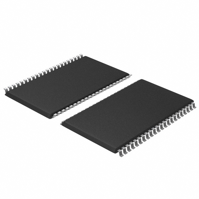
- Part No.:
- CY62157EV30LL-55ZSXET
- Manufacturer:
- Infineon Technologies
- Category:
- Memory
- Package:
- 44-TSOP (0.400", 10.16mm Width)
- Datasheet:
-
 CY62157EV30LL-55ZSXET.pdf
- Description:
- IC SRAM 8MBIT PARALLEL 44TSOP II
- Quantity:
- Payment:

- Shipping:

Inventory:2,937
Please send an inquiry. Send us your inquiry, and we will respond immediately.
Product details
Overview
CY62157EV30LL-55ZSXET from Infineon Technologies (formerly Cypress) is a 8-Mbit MoBL® CMOS static RAM organized as 512K × 16, operating at 2.2–3.6 V with 55 ns access time for Automotive-E grade (–40 °C to +125 °C). It delivers ultra-low standby current (2 µA typical, 30 µA max), active current of 1.8 mA at 1 MHz, and supports byte-wide or word-wide access via BHE/ BLE controls. Used in automotive infotainment head units requiring non-volatile data buffering during power transitions.
For engineers reviewing the CY62157EV30LL-55ZSXET datasheet, CY62157EV30LL-55ZSXET pinout, CY62157EV30LL-55ZSXET application, or CY62157EV30LL-55ZSXET equivalent, key selection criteria include its dual-configurable memory organization (512K × 16 / 1M × 8), automatic power-down on chip deselect, TSOP I package compatibility, and guaranteed operation up to +125 °C ambient.
Technical Context
This SRAM implements a fully static CMOS architecture with independent byte enable (BHE/ BLE) control, enabling selective 8-bit writes without disturbing adjacent bytes. Its power-down circuitry activates when CE1 is HIGH, CE2 is LOW, or both BHE and BLE are HIGH - reducing ICCDR to ≤30 µA at 1.5 V retention voltage.
The device supports two physical configurations: as a 512K × 16 SRAM (BYTE pin tied HIGH in 48-pin TSOP I) or as a 1M × 8 SRAM (BYTE pin LOW, repurposing A19 on pin 45). Addressing uses 19 address lines (A0–A18), with no internal refresh required and full compatibility with standard asynchronous SRAM controllers.
Key Specifications
| Parameter | Value and Actual Design Meaning |
|---|---|
| Memory Size | 8 Mbit (512K × 16 or 1M × 8 configurable) |
| Access Time | 55 ns max at –40 °C to +125 °C (Automotive-E grade) |
| VCC Range | 2.20 V to 3.60 V - supports single-supply battery-backed systems |
| Standby Current | 30 µA max at +125 °C - enables long-term data retention in always-on modules |
| Active Current | 1.8 mA typical at f = 1 MHz - minimizes thermal load in dense PCB layouts |
| Data Retention Voltage | 1.5 V min - allows backup from supercapacitors or low-voltage energy harvesters |
| Operating Temperature | –40 °C to +125 °C - qualified for under-hood automotive electronics |
Pinout & Package
Package: 48-pin Thin Small Outline Package (TSOP I), RoHS-compliant, lead-free, surface-mountable with 0.5 mm pitch.
| Pin/Terminal | Circuit Role | Design Meaning |
|---|---|---|
| A0–A18 | Address Inputs | 19-bit address bus supporting full 512K-word addressing; A19 used only in 1M×8 mode |
| I/O0–I/O7 | Data Bus (Low Byte) | Bi-directional 8-bit data path enabled when BLE = LOW; high-impedance when deselected |
| I/O8–I/O15 | Data Bus (High Byte) | Bi-directional 8-bit data path enabled when BHE = LOW; isolated during byte-write operations |
| CE1 / CE2 | Chip Enable Inputs | Dual CE logic: device active only when CE1 = LOW AND CE2 = HIGH; enables hierarchical memory decoding |
| OE | Output Enable | Controls output drivers only - does not affect internal state or power mode |
| WE | Write Enable | Active-LOW write strobe; initiates write cycle when CE1/CE2 active and WE falls |
| BHE / BLE | Byte Enable Controls | Independent gating of high/low data bytes - enables partial writes without read-modify-write overhead |
| VCC / VSS | Power / Ground | Dual VCC pins (pins 24 & 48) and dual VSS pins (pins 23 & 47) reduce IR drop and improve noise immunity |
Key Features
| Feature | Design Value |
|---|---|
| Configurable Organization | Hardware-selectable 512K × 16 or 1M × 8 mode via BYTE pin - eliminates need for external multiplexing logic |
| Automatic Power-Down | Enters ultra-low-power state when CE1 HIGH, CE2 LOW, or both BHE/ BLE HIGH - no software or timing control needed |
| CMOS-Compatible Interface | VIH/VIL thresholds scale with VCC (e.g., VIH ≥ 2.2 V at 2.7–3.6 V) - ensures robust operation across supply tolerance |
| High-Z Output Control | Outputs enter high-impedance within 10 ns of OE/CE/BHE/ BLE deactivation - prevents bus contention in multi-SRAM systems |
| Automotive Qualification | AEC-Q100 Grade 2 compliant (–40 °C to +105 °C) and extended to +125 °C per datasheet - validated for engine control modules |
Applications
| Automotive Instrument Clusters | ADAS Sensor Fusion Units |
|---|---|
|
Use Scenario: Real-time storage of gauge rendering buffers and CAN message history during ignition cycling. IC Role / Device Role / Timing Role: Asynchronous SRAM buffer between MCU and TFT controller, holding frame metadata and calibration offsets. Use Value: 55 ns access time ensures pixel pipeline continuity; 30 µA standby current preserves content across stop-start cycles without backup battery. |
Use Scenario: Temporary aggregation of radar, camera, and ultrasonic sensor timestamps before fusion algorithm execution. IC Role / Device Role / Timing Role: Low-latency shared memory for heterogeneous processor clusters performing time-critical sensor alignment. Use Value: Dual-byte enable allows parallel timestamp writes from multiple sensor interfaces; +125 °C rating supports placement near radar MMICs. |
| Telematics Control Units (TCU) | Electric Vehicle Battery Management Systems |
|
Use Scenario: Storing encrypted cellular modem firmware patches and OTA update staging area in disconnected mode. IC Role / Device Role / Timing Role: Secure, fast-access scratchpad memory for cryptographic acceleration engines during firmware validation. Use Value: 1.5 V data retention enables operation during brown-out events; pin-compatible upgrade path from CY62157DV30 simplifies legacy design refresh. |
Use Scenario: Caching cell voltage and temperature sampling history for predictive SOC/SOH algorithms during charging pauses. IC Role / Device Role / Timing Role: High-reliability buffer between analog front-end ADCs and ARM Cortex-R5 safety core. Use Value: Dual VCC/VSS pins minimize ground bounce in noisy high-current environments; automotive-grade qualification ensures ASIL-B compliance support. |
Equivalent & Alternatives
The following parts are listed as comparable options for similar high-speed, low-power SRAM applications.
| Alternative Part | Technical Difference | Application Difference | Selection Advice |
|---|---|---|---|
| IS61WV51216EDBLL-55TLI | 55 ns access, +85 °C max, 3.3 V only, no BYTE pin or 1M×8 mode | Limited to industrial temp range; lacks automotive qualification and dual-organization flexibility | Select if cost-sensitive industrial designs require identical speed but do not need extended temperature or configuration options |
| AS6C4008-55ZIN | 55 ns access, +85 °C max, 2.7–3.6 V, single CE, no BHE/ BLE | No byte-enable control; requires external logic for partial writes; no automotive qualification | Choose for simple, low-pin-count embedded systems where full 16-bit writes suffice and thermal margin is adequate |
Compared with IS61WV51216EDBLL-55TLI and AS6C4008-55ZIN, CY62157EV30LL-55ZSXET uniquely combines +125 °C operation, hardware-configurable organization, and true dual-byte enable - making it the only option qualified for under-hood ADAS and battery management subsystems requiring deterministic low-power behavior.
Availability
CY62157EV30LL-55ZSXET is available at Aetrix Electronics and suitable for automotive instrument clusters, ADAS sensor fusion units, and telematics control units requiring stable component supply across extended temperature ranges and long product lifecycles.
Supply support for CY62157EV30LL-55ZSXET includes scheduled delivery planning, volume procurement assistance, BOM continuity management, traceable sourcing, and lifecycle availability coordination for OEM customers, industrial embedded developers, connected-device designers, and electronics production programs.
Manufacturer
Infineon Technologies is a global semiconductor leader headquartered in Munich, Germany, specializing in power systems, automotive microcontrollers, and memory solutions acquired from Cypress Semiconductor.
CY62157EV30 belongs to the MoBL® (More Battery Life™) SRAM product line, engineered specifically for ultra-low-power, high-reliability applications in automotive and industrial edge devices where data integrity and thermal resilience are critical.
FAQ
What is the maximum junction temperature for CY62157EV30LL-55ZSXET?
The device is rated for operation up to +125 °C ambient temperature (Automotive-E grade), with thermal resistance θJA = 60.07 °C/W in 48-pin TSOP I. Maximum junction temperature is calculated as TJ = TA + (θJA × PD); at 30 µA standby current and 3.6 V, power dissipation remains below 0.11 mW, keeping TJ well within safe limits even at full ambient rating.
Can CY62157EV30LL-55ZSXET be used in 1M × 8 mode on a board designed for 512K × 16?
Yes - the 48-pin TSOP I package supports hardware reconfiguration: tie the BYTE pin LOW to enable 1M × 8 mode, which repurposes pin 45 as A19 and disables BHE, BLE, and I/O8–I/O14. No PCB redesign is needed beyond the BYTE pin connection; all other signals retain identical mapping and timing.
Does CY62157EV30LL-55ZSXET require an external clock or refresh signal?
No - it is a fully static CMOS SRAM with no clock input or refresh requirement. Data retention is maintained as long as VCC remains ≥1.5 V and chip enable conditions meet ISB2 specifications. All timing is asynchronous and controlled solely by CE, OE, WE, and BHE/ BLE edges.
How does the automatic power-down feature activate without firmware intervention?
Power-down triggers automatically when any of these conditions occur: CE1 HIGH, CE2 LOW, or both BHE and BLE HIGH. The internal circuit monitors these inputs continuously - no register writes, timers, or CPU involvement are required. Exit occurs within 0 ns tPU (power-up time) when valid CE/WE/OE conditions resume.
CY62157EV30LL-55ZSXET Specifications
- Product attributes
- Attribute value
- Manufacturer:
- Infineon Technologies
- Series:
- MOBL™
- Package/Case:
- 44-TSOP (0.400", 10.16mm Width)
- Packaging:
- Tape & Reel (TR)
- Product Status:
- Active
- Programmable:
- Not Verified
- Memory Type:
- Volatile
- Memory Format:
- SRAM
- Technology:
- SRAM - Asynchronous
- Memory Size:
- 8Mbit
- Memory Organization:
- 512K x 16
- Memory Interface:
- Parallel
- Clock Frequency:
- -
- Write Cycle Time - Word, Page:
- 55ns
- Access Time:
- 55 ns
- Voltage - Supply:
- 2.2V ~ 3.6V
- Operating Temperature:
- -40°C ~ 125°C (TA)
- Grade:
- -
- Qualification:
- -
- Mounting Type:
- Surface Mount
- Supplier Device Package:
- 44-TSOP II
CY62157EV30LL-55ZSXET FAQ
1.How can I place an order for CY62157EV30LL-55ZSXET through Aetrix?
Please submit a Request for Quotation (RFQ) for CY62157EV30LL-55ZSXET on Aetrix. Our sales agent will provide a competitive quotation and guide you through the order confirmation once you accept the terms.
2.Are the price and stock information for CY62157EV30LL-55ZSXET reliable?
The price and inventory of CY62157EV30LL-55ZSXET are updated periodically and may fluctuate due to market conditions. Stock and pricing data are typically refreshed every 24 hours. Quotation validity for CY62157EV30LL-55ZSXET is usually 5 days.
3.What payment methods are accepted for CY62157EV30LL-55ZSXET?
We accept Wire Transfer, PayPal, Credit Card, Western Union, MoneyGram, and Escrow for CY62157EV30LL-55ZSXET transactions.
Note: Certain payment methods may incur a processing fee.
4.How is shipping managed for CY62157EV30LL-55ZSXET?
CY62157EV30LL-55ZSXET orders can be shipped via leading logistics carriers, including DHL, UPS, FedEx, TNT, or Registered Mail.
Once your CY62157EV30LL-55ZSXET order is processed, you will receive an email with the shipment details and tracking number.
Note: Tracking information may take up to 24 hours to appear. Express delivery typically takes 3–5 business days.
5.How can I obtain technical support or documentation for CY62157EV30LL-55ZSXET?
For technical support, including CY62157EV30LL-55ZSXET datasheets, pinout diagrams, or application guidance, please contact our engineering support team. They can provide detailed documentation and assistance for your CY62157EV30LL-55ZSXET requirements.
6.How does Aetrix verify that CY62157EV30LL-55ZSXET is sourced from the original manufacturer or authorized distributors?
All CY62157EV30LL-55ZSXET products on Aetrix are procured from qualified distributors and authorized channels. Our dedicated quality assurance team conducts strict verification, including traceability checks and, if necessary, third-party testing. This ensures that CY62157EV30LL-55ZSXET meets industry standards.
7.What is the process for return or replacement of CY62157EV30LL-55ZSXET?
All CY62157EV30LL-55ZSXET units undergo pre-shipment inspection (PSI). If there is an issue with CY62157EV30LL-55ZSXET, returns or replacements are accepted under the following conditions:
1.Quantity discrepancies, incorrect items, or visible external defects (such as breakage or corrosion), acknowledged by Aetrix.
2.The issue is reported within 90 days of delivery.
3.The CY62157EV30LL-55ZSXET part is unused and in its original packaging.
Return procedure for CY62157EV30LL-55ZSXET:
1.Submit a request within 90 days.
2.Obtain a Return Material Authorization (RMA) from Aetrix.
CY62157EV30LL-55ZSXET Tags

-
M24C02-WMN6TP
STMicroelectronics

-
AT24C02C-XHM-T
Microchip Technology

-
AT21CS01-STUM10-T
Microchip Technology

-
AT24C02C-SSHM-T
Microchip Technology

-
24LC01BT-I/OT
Microchip Technology

-
M24C02-FMC6TG
STMicroelectronics
-
AT24CS02-SSHM-T
Microchip Technology

-
93LC46BT-I/OT
Microchip Technology
-
AT24C04C-SSHM-T
Microchip Technology

-
24LC01BT-I/SN
Microchip Technology
-
24AA02UIDT-I/OT
Microchip Technology

-
AT24C08C-STUM-T
Microchip Technology
Tech Hub

The 74HC595 uses push-pull logic outputs, while the TPIC6B595 uses 50 V open-drain DMOS sinks for higher-power loads. This guide compares timing, current limits, 3.3 V interfacing, load wiring, thermal…

The 74HC595 converts serial data into eight stable parallel outputs. This guide covers pin functions, shift and storage timing, OE and MR behavior, drive-current limits, cascading, voltage compatibilit…

A technical comparison of level-sensitive latches and edge-triggered flip-flops, covering timing windows, setup and hold limits, master–slave operation, time borrowing, race-through, HDL inference and…

A D latch stores one bit while Enable controls when data can pass. This reference covers gate-level operation, truth tables, transparency, setup and hold timing, LE versus OE, common ICs and practical …

An SR latch stores one bit through cross-coupled feedback. This engineering reference covers NOR and NAND implementations, truth tables, forbidden-state recovery, gated operation, switch debouncing, fa…

Latch circuits retain one bit through feedback. This technical reference covers SR and D latches, truth tables, transparency, timing limits, latch-versus-flip-flop behavior, applications and common log…

An engineering guide to LED driver operation, constant-current and constant-voltage outputs, linear and switching topologies, dimming, IC selection, calculations, replacement compatibility, and fault c…

Operational amplifier guide covering op amp basics, feedback, ideal vs real op amps, common configurations, buffer circuits, offset, bias current, gain-bandwidth, slew rate, rail-to-rail limits and sel…

Jumper cables guide covering safe connection order, red and black clamp placement, final ground connection, cable gauge, length, clamp quality, copper vs CCA cables, jump starter comparison and battery…

LDO regulator guide covering low dropout voltage, power dissipation, thermal design, PSRR, output noise, capacitor stability, adjustable LDO circuits, LDO vs buck converter and datasheet selection chec…


