
 My Inquiry
 My Account


Infineon Technologies CY62162G30-45BGXIT
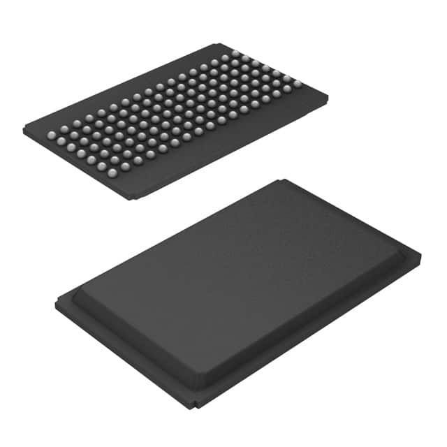
- Part No.:
- CY62162G30-45BGXIT
- Manufacturer:
- Infineon Technologies
- Category:
- Memory
- Package:
- 119-BGA
- Datasheet:
-
 CY62162G30-45BGXIT.pdf
- Description:
- IC SRAM 16MBIT PARALLEL 119PBGA
- Quantity:
- Payment:

- Shipping:

Inventory:3,121
Please send an inquiry. Send us your inquiry, and we will respond immediately.
Product details
Overview
CY62162G30-45BGXIT from Infineon Technologies (formerly Cypress) is a 16-Mbit MoBL® SRAM organized as 512K × 32 bits with embedded single-bit error-correcting code (ECC), 45 ns access time, 1.65–3.6 V dual-voltage operation, and ultra-low 5.5 µA typical standby current. It serves as a high-reliability, low-power data buffer in portable industrial controllers requiring ECC protection and battery longevity.
For engineers reviewing the CY62162G30-45BGXIT datasheet, CY62162G30-45BGXIT pinout, CY62162G30-45BGXIT application, or CY62162G30-45BGXIT equivalent, key selection criteria include ECC-enabled single-bit correction, dual chip enable (CE1/CE2) for memory expansion, ERR output assertion on correction, 119-ball PBGA package compatibility, and automatic power-down mode reducing active current by >99% when deselected.
Technical Context
This SRAM implements a CMOS-based 512K × 32-bit array with dedicated ECC encoder/decoder circuitry that detects and corrects single-bit errors during read operations without host intervention. The ERR pin asserts HIGH only upon successful single-bit correction - no automatic write-back is performed.
It supports four independent byte enables (BA–BD) for granular 8-bit writes across I/O0–I/O31, and features dual chip enables (CE1 active-low, CE2 active-high) enabling seamless bank expansion. Standby is entered when CE1 is HIGH, CE2 is LOW, or any byte enable is HIGH, placing all I/Os in high-impedance state.
Key Specifications
| Parameter | Value and Actual Design Meaning |
|---|---|
| Memory Size | 16 Mbit (512K × 32 bits) - provides 2 MB of byte-addressable storage with 32-bit parallel interface |
| Access Time | 45 ns at 2.2–3.6 V - ensures deterministic timing for real-time control loops running ≤22.2 MHz |
| ECC Function | Single-bit error detection and correction per 32-bit word - improves system reliability without software overhead |
| Standby Current | 5.5 µA typical (max 16 µA) - enables multi-year battery life in always-on sensor nodes |
| Supply Voltage | 1.65–2.2 V or 2.2–3.6 V - supports direct interfacing with 1.8 V or 3.3 V logic domains |
| Data Retention | 1.0 V minimum - maintains stored data during brown-out or deep-sleep modes |
| Package | 119-ball PBGA (10 mm × 13 mm, 0.8 mm pitch) - center-power/ground layout reduces noise and improves thermal dissipation |
Pinout & Package
The CY62162G30-45BGXIT is housed in a 119-ball plastic ball grid array (PBGA) package with center power/ground ball placement to minimize IR drop and improve signal integrity. Pin functions are validated per Infineon Document 001-81598 Rev. *F (Pages 5–6).
| Pin/Terminal | Circuit Role | Design Meaning |
|---|---|---|
| A0–A18 | Address Inputs | 19-bit address bus supporting full 512K-word addressing; TTL-compatible thresholds |
| I/O0–I/O31 | Bi-directional Data Bus | 32-bit parallel interface with high-impedance tri-state control via CE/OE/BE |
| BA–BD | Byte Enable Inputs | Four independent 8-bit write masks - enables partial-word writes without read-modify-write |
| CE1, CE2 | Chip Enables | Dual-enable logic (CE1 active-low, CE2 active-high) allows daisy-chained or interleaved memory banks |
| WE, OE | Write/Output Enables | Asynchronous control: WE LOW + CE active = write; OE LOW + CE active = read |
| ERR | Error Indication Output | Open-drain HIGH pulse signals successful single-bit correction - requires external pull-up |
| VCC, GND | Power/Termination | Multiple distributed VCC/GND balls (center-aligned) reduce impedance and EMI in high-speed operation |
Key Features
| Feature | Design Value |
|---|---|
| Embedded ECC Engine | Hardware-accelerated single-bit correction per 32-bit word - eliminates need for software ECC routines and associated latency |
| Ultra-Low Standby Power | 5.5 µA typical ISB2 - extends battery life in portable medical monitors and handheld test equipment |
| Dual-Voltage Operation | 1.65–2.2 V and 2.2–3.6 V ranges - simplifies integration with mixed-voltage SoCs and legacy 3.3 V peripherals |
| Automatic Power-Down Mode | Reduces ICC by >99% when CE/BE inactive - triggered without host command, ideal for intermittent sensing applications |
| TTL-Compatible I/O | VIH/VIL thresholds match standard 1.8 V and 3.3 V logic families - eliminates level-shifter requirements |
Applications
| Industrial PLC Data Buffer | Portable Medical Monitor Memory |
|---|---|
|
Use Scenario: Stores real-time sensor logs and configuration parameters in DIN-rail mounted programmable logic controllers operating continuously in harsh environments. IC Role / Device Role / Timing Role: Non-volatile shadow RAM holding critical runtime variables; ECC prevents silent data corruption from EMI-induced bit flips. Use Value: Eliminates periodic checksum validation overhead while ensuring deterministic 45 ns read/write response for motion control interrupts. |
Use Scenario: Holds patient waveform history and calibration coefficients in battery-powered ECG and SpO₂ devices with multi-week operational life. IC Role / Device Role / Timing Role: Low-power SRAM buffer between ADC and microcontroller; 1.0 V data retention preserves memory during sleep cycles. Use Value: 5.5 µA standby current enables >3 years of shelf life; ERR pin alerts firmware to correct memory errors before clinical data export. |
| Automotive ADAS Sensor Hub | Smart Meter Firmware Cache |
|
Use Scenario: Caches radar preprocessing results and CAN message buffers in automotive vision systems operating across –40 °C to +105 °C ambient. IC Role / Device Role / Timing Role: High-reliability scratchpad memory for real-time image feature extraction; dual-voltage support interfaces with 1.8 V ISP and 3.3 V CAN transceivers. Use Value: 119-ball PBGA's thermal resistance (θJA = 20.92 °C/W) sustains performance under engine-bay temperature cycling. |
Use Scenario: Stores tariff tables, encryption keys, and usage logs in utility smart meters deployed in unattended outdoor enclosures. IC Role / Device Role / Timing Role: Secure, tamper-resilient memory with ECC-protected firmware metadata; ERR flag triggers secure erase on repeated correction events. Use Value: Single-bit ECC prevents undetected corruption of billing data over 15+ year field lifetime without maintenance intervention. |
Equivalent & Alternatives
The following parts are listed as comparable options for similar ECC SRAM applications.
| Alternative Part | Technical Difference | Application Difference | Selection Advice |
|---|---|---|---|
| ISSI IS61WV102432BLL-10MLI | No integrated ECC; requires external error-handling logic; 10 ns faster (10 ns access), but higher 25 mA ICC | Lacks hardware-level error correction - unsuitable where silent data corruption must be prevented without CPU involvement | Select only if speed outweighs reliability needs and host processor can implement software ECC |
| Micron MT47H64M4BQ-37E:H | DDR2 SDRAM (not SRAM); requires refresh controller; 64 Mbit density; no built-in ECC (requires chipset-level ECC) | Higher bandwidth but incompatible timing model - not drop-in replaceable due to synchronous interface and command protocol | Choose only for high-throughput streaming applications where burst access and external memory controller are available |
Compared with IS61WV102432BLL-10MLI and MT47H64M4BQ-37E:H, CY62162G30-45BGXIT uniquely delivers autonomous single-bit correction in an asynchronous SRAM interface with sub-µA standby - essential for safety-critical, battery-constrained, or maintenance-free deployments.
Availability
CY62162G30-45BGXIT is available at Aetrix Electronics and suitable for industrial PLC data buffering, portable medical monitor memory, automotive ADAS sensor hubs, and smart meter firmware caching requiring stable component supply across extended product lifecycles.
Supply support for CY62162G30-45BGXIT includes scheduled delivery planning, volume procurement assistance, BOM continuity management, traceable sourcing, and lifecycle availability coordination for OEM customers, industrial embedded developers, connected-device designers, and electronics production programs.
Manufacturer
Infineon Technologies is a global semiconductor leader headquartered in Munich, Germany, specializing in power management, sensing, connectivity, and security solutions for industrial, automotive, and IoT markets.
CY62162G30-45BGXIT belongs to Infineon's MoBL® (More Battery Life™) SRAM product line, engineered specifically for ultra-low-power, high-reliability embedded systems where ECC-protected memory and nanowatt standby operation are mandatory.
FAQ
Does CY62162G30-45BGXIT support automatic write-back after ECC correction?
No. The device detects and corrects single-bit errors during read operations and asserts the ERR pin, but it does not perform automatic write-back to memory. Host firmware must initiate a write cycle if persistent correction is required. This design minimizes unintended writes and preserves memory endurance in battery-operated systems.
What is the function of the ERR pin, and how should it be terminated?
The ERR pin is an open-drain output that drives HIGH only when a single-bit error is detected and corrected during a read cycle. It must be externally pulled up to VCC via a 4.7 kΩ resistor. Leaving ERR floating is acceptable if error monitoring is unused, per datasheet Note 4.
Can CY62162G30-45BGXIT operate reliably at 1.65 V supply?
Yes. The device is fully specified for 1.65–2.2 V operation, with 55 ns access time guaranteed at 1.65 V. At this voltage, typical standby current is 7 µA (max 26 µA), and data retention holds down to 1.0 V - making it suitable for energy-harvesting and ultra-low-voltage designs.
How does the dual chip enable (CE1/CE2) simplify memory expansion?
CE1 (active-low) and CE2 (active-high) allow two independent enable conditions: CE1=LOW + CE2=HIGH enables the device, while other combinations disable it. This permits hierarchical decoding - e.g., using CE2 to select a memory bank and CE1 to select individual chips within that bank - reducing address decoder complexity in multi-MB systems.
CY62162G30-45BGXIT Specifications
- Product attributes
- Attribute value
- Manufacturer:
- Infineon Technologies
- Series:
- MOBL™
- Package/Case:
- 119-BGA
- Packaging:
- Tape & Reel (TR)
- Product Status:
- Last Time Buy
- Programmable:
- Not Verified
- Memory Type:
- Volatile
- Memory Format:
- SRAM
- Technology:
- SRAM - Asynchronous
- Memory Size:
- 16Mbit
- Memory Organization:
- 512K x 32
- Memory Interface:
- Parallel
- Clock Frequency:
- -
- Write Cycle Time - Word, Page:
- 45ns
- Access Time:
- 45 ns
- Voltage - Supply:
- 1.65V ~ 2.2V
- Operating Temperature:
- -40°C ~ 85°C (TA)
- Grade:
- -
- Qualification:
- -
- Mounting Type:
- Surface Mount
- Supplier Device Package:
- 119-PBGA (14x22)
CY62162G30-45BGXIT FAQ
1.How can I place an order for CY62162G30-45BGXIT through Aetrix?
Please submit a Request for Quotation (RFQ) for CY62162G30-45BGXIT on Aetrix. Our sales agent will provide a competitive quotation and guide you through the order confirmation once you accept the terms.
2.Are the price and stock information for CY62162G30-45BGXIT reliable?
The price and inventory of CY62162G30-45BGXIT are updated periodically and may fluctuate due to market conditions. Stock and pricing data are typically refreshed every 24 hours. Quotation validity for CY62162G30-45BGXIT is usually 5 days.
3.What payment methods are accepted for CY62162G30-45BGXIT?
We accept Wire Transfer, PayPal, Credit Card, Western Union, MoneyGram, and Escrow for CY62162G30-45BGXIT transactions.
Note: Certain payment methods may incur a processing fee.
4.How is shipping managed for CY62162G30-45BGXIT?
CY62162G30-45BGXIT orders can be shipped via leading logistics carriers, including DHL, UPS, FedEx, TNT, or Registered Mail.
Once your CY62162G30-45BGXIT order is processed, you will receive an email with the shipment details and tracking number.
Note: Tracking information may take up to 24 hours to appear. Express delivery typically takes 3–5 business days.
5.How can I obtain technical support or documentation for CY62162G30-45BGXIT?
For technical support, including CY62162G30-45BGXIT datasheets, pinout diagrams, or application guidance, please contact our engineering support team. They can provide detailed documentation and assistance for your CY62162G30-45BGXIT requirements.
6.How does Aetrix verify that CY62162G30-45BGXIT is sourced from the original manufacturer or authorized distributors?
All CY62162G30-45BGXIT products on Aetrix are procured from qualified distributors and authorized channels. Our dedicated quality assurance team conducts strict verification, including traceability checks and, if necessary, third-party testing. This ensures that CY62162G30-45BGXIT meets industry standards.
7.What is the process for return or replacement of CY62162G30-45BGXIT?
All CY62162G30-45BGXIT units undergo pre-shipment inspection (PSI). If there is an issue with CY62162G30-45BGXIT, returns or replacements are accepted under the following conditions:
1.Quantity discrepancies, incorrect items, or visible external defects (such as breakage or corrosion), acknowledged by Aetrix.
2.The issue is reported within 90 days of delivery.
3.The CY62162G30-45BGXIT part is unused and in its original packaging.
Return procedure for CY62162G30-45BGXIT:
1.Submit a request within 90 days.
2.Obtain a Return Material Authorization (RMA) from Aetrix.
CY62162G30-45BGXIT Tags

-
M24C02-WMN6TP
STMicroelectronics

-
AT24C02C-XHM-T
Microchip Technology

-
AT21CS01-STUM10-T
Microchip Technology

-
AT24C02C-SSHM-T
Microchip Technology

-
24LC01BT-I/OT
Microchip Technology

-
M24C02-FMC6TG
STMicroelectronics
-
AT24CS02-SSHM-T
Microchip Technology

-
93LC46BT-I/OT
Microchip Technology
-
AT24C04C-SSHM-T
Microchip Technology

-
24LC01BT-I/SN
Microchip Technology
-
24AA02UIDT-I/OT
Microchip Technology

-
AT24C08C-STUM-T
Microchip Technology
Tech Hub

The 74HC595 converts serial data into eight stable parallel outputs. This guide covers pin functions, shift and storage timing, OE and MR behavior, drive-current limits, cascading, voltage compatibilit…
A technical comparison of level-sensitive latches and edge-triggered flip-flops, covering timing windows, setup and hold limits, master–slave operation, time borrowing, race-through, HDL inference and…
A D latch stores one bit while Enable controls when data can pass. This reference covers gate-level operation, truth tables, transparency, setup and hold timing, LE versus OE, common ICs and practical …

An SR latch stores one bit through cross-coupled feedback. This engineering reference covers NOR and NAND implementations, truth tables, forbidden-state recovery, gated operation, switch debouncing, fa…

Latch circuits retain one bit through feedback. This technical reference covers SR and D latches, truth tables, transparency, timing limits, latch-versus-flip-flop behavior, applications and common log…

An engineering guide to LED driver operation, constant-current and constant-voltage outputs, linear and switching topologies, dimming, IC selection, calculations, replacement compatibility, and fault c…

Operational amplifier guide covering op amp basics, feedback, ideal vs real op amps, common configurations, buffer circuits, offset, bias current, gain-bandwidth, slew rate, rail-to-rail limits and sel…

Jumper cables guide covering safe connection order, red and black clamp placement, final ground connection, cable gauge, length, clamp quality, copper vs CCA cables, jump starter comparison and battery…

LDO regulator guide covering low dropout voltage, power dissipation, thermal design, PSRR, output noise, capacitor stability, adjustable LDO circuits, LDO vs buck converter and datasheet selection chec…

Conditional Access Module guide covering CAM meaning, CI/CI+ interface, smart card authorization, DVB security workflow, TV and set-top box compatibility, internal electronics, ESD protection, connecto…


