
 My Inquiry
 My Account


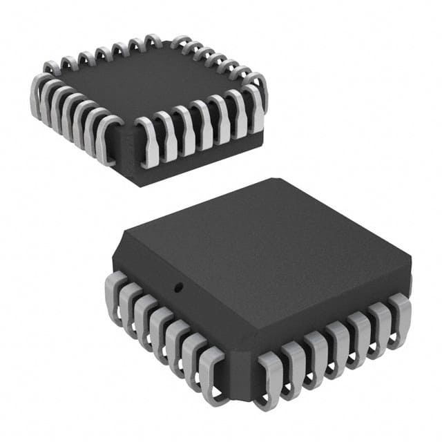
Cypress Semiconductor Corp CY7B9234-270JXC
- Part No.:
- CY7B9234-270JXC
- Manufacturer:
- Cypress Semiconductor Corp
- Category:
- Drivers, Receivers, Transceivers
- Package:
- -
- Datasheet:
-
 CY7B9234-270JXC.pdf
- Description:
- SMPTE HOTLINK TRANSMITTER/RECEIV
- Quantity:
- Payment:

- Shipping:

Inventory:355
Please send an inquiry. Send us your inquiry, and we will respond immediately.
Product details
Overview
CY7B9234-270JXC from Cypress Semiconductor is an SMPTE HOTLink® transmitter IC compliant with SMPTE-259M-CD, DVB-ASI, and Fibre Channel standards. It performs 8B/10B encoding or bypasses encoding, delivers triple PECL 100K serial outputs at 270 Mbps, operates on a single +5V supply, and integrates PLL clock generation without external components - enabling uncompressed SD-SDI video transmission over fiber, coax, or twisted pair in broadcast infrastructure.
For engineers reviewing the CY7B9234-270JXC datasheet, CY7B9234-270JXC pinout, CY7B9234-270JXC application, or CY7B9234-270JXC equivalent, key selection criteria include SMPTE-259M-CD compliance, 270 Mbps serial data rate, TTL-synchronous parallel interface, built-in BIST capability, and PLCC-28 packaging for legacy broadcast equipment design and repair.
Technical Context
The CY7B9234-270JXC implements a fully integrated transmitter architecture with a byte-rate input clock (CKW), parallel 8-bit TTL data path (D0–D7), and three differential PECL serial outputs (OUTA±, OUTB±, OUTC±). Its internal PLL multiplies CKW to generate the 2.7 GHz bit clock required for 270 Mbps operation (10× byte rate).
Encoding mode is selected via the MODE pin: grounded for 8B/10B encoding, VCC for unencoded 10-bit pass-through (Da–Dj), or floating for factory test mode where OUTA+/OUTB+ serve as differential bit clock outputs. The FOTO pin enables optical transmitter shutdown without disrupting OUTC± loopback diagnostics.
Key Specifications
| Parameter | Value and Actual Design Meaning |
|---|---|
| Data Rate | 270 Mbps - matches SMPTE-259M standard for 480i/576i SD-SDI video transport. |
| Encoding Mode | Configurable 8B/10B or 10-bit unencoded - supports both SMPTE scrambling and DVB-ASI protocols. |
| Output Interface | Triple PECL 100K differential outputs - directly drives fiber-optic transmitters, coax drivers, or terminated PCB traces. |
| Power Consumption | 350 mW typical - enables thermal management in dense broadcast router card designs. |
| Supply Voltage | +5V single supply - eliminates need for dual-rail or LDO sequencing in legacy video systems. |
| Input Interface | TTL-synchronous parallel (D0–D7, CKW, ENA/ENN) - interfaces natively with FIFOs (e.g., CY7C42X) and SMPTE controllers (CY7C9235). |
| Built-In Self-Test | Hardware BIST generator and checker - validates transmitter, link, and receiver functionality without external pattern generators. |
Pinout & Package
Package: 28-pin Plastic Leaded Chip Carrier (PLCC), 11.43 mm × 11.43 mm, JEDEC MS-026AC, lead-free compatible (per Rev. *B datasheet).
| Pin | Circuit Role | Design Meaning |
|---|---|---|
| D0–D7 | Parallel Data Input | TTL inputs accepting 8-bit video or protocol data on rising CKW edge when ENA/ENN asserted. |
| CKW | Byte-Rate Clock Input | Drives internal PLL to generate 2.7 GHz serial clock; must be crystal-referenced within ±100 ppm. |
| ENA / ENN | Data Enable Control | Asynchronous enable signals controlling byte loading; dual-enable allows flexible handshaking with host logic. |
| FOTO | Fiber-Optic Disable | Asserting HIGH forces OUTA±/OUTB± to logic zero, extinguishing optical output while preserving OUTC± for loopback. |
| MODE | Encoding Mode Select | GND = 8B/10B encode; VCC = unencoded 10-bit pass-through; floating = test clock output mode. |
| OUTA± / OUTB± / OUTC± | Differential Serial Outputs | PECL 100K outputs; OUTC± unaffected by FOTO - used for board-level diagnostic loopback. |
| BISTEN | Self-Test Enable | Activates alternating 1–0 pattern (D10.2/D21.5) or full-link BIST sequence when ENA/ENN high. |
Key Features
| Feature | Design Value |
|---|---|
| SMPTE-259M-CD Compliance | Guarantees interoperability with broadcast-grade SD-SDI infrastructure including routers, switchers, and recorders. |
| No External PLL Components | Reduces bill-of-materials count and layout complexity - eliminates discrete VCOs, loop filters, and reference dividers. |
| Triple Independent PECL Outputs | Enables redundant link paths or simultaneous distribution to multiple receivers without external fanout buffers. |
| Hardware BIST with Link Validation | Performs end-to-end functional verification of transmitter, physical medium, and receiver in under 1 ms per test cycle. |
| FOTO-Controlled Optical Shutdown | Allows safe hot-plug of fiber modules and power-gating of unused links without disrupting system clock domain. |
Applications
| SD-SDI Video Router | Broadcast Video Recorder |
|---|---|
|
Use Scenario: High-density SD-SDI routing matrix handling 32+ video sources with frame-accurate switching. IC Role / Device Role / Timing Role: Transmitter converting parallel video data from FPGA-based switch fabric into SMPTE-259M-compliant serial streams. Use Value: Triple PECL outputs drive multiple downstream destinations; BIST enables automated pre-deployment link validation. |
Use Scenario: Embedded recording engine capturing uncompressed 480i/576i video from camera feeds. IC Role / Device Role / Timing Role: Serializer interfacing between video processing ASIC and coaxial SDI output stage. Use Value: 270 Mbps fixed-rate operation ensures deterministic latency; TTL interface simplifies timing closure with video FIFOs. |
| Video Editing Workstation I/O | Studio Monitor Distribution Hub |
|
Use Scenario: PCIe-based capture/playback card supporting real-time editing of SD-SDI timelines. IC Role / Device Role / Timing Role: Parallel-to-serial bridge between host memory controller and SDI PHY layer. Use Value: MODE pin configures unencoded mode for proprietary metadata channels; RP output synchronizes with CY7C42X FIFO read clocks. |
Use Scenario: Centralized monitor feed distributor sending identical SD-SDI signals to 8+ on-set displays. IC Role / Device Role / Timing Role: Fanout transmitter replicating one video source across multiple PECL outputs. Use Value: OUTC± remains active during FOTO assertion - enables continuous loopback monitoring while other outputs are disabled. |
Equivalent & Alternatives
The following parts are listed as comparable options for similar SMPTE-259M transmitter applications.
| Alternative Part | Technical Difference | Application Difference | Selection Advice |
|---|---|---|---|
| LMH0303SQ/NOPB | Single-channel, 3G-SDI capable (up to 2.97 Gbps); requires external clock synthesis; LVDS output. | Supports HD-SDI and 3G-SDI; not SMPTE-259M-CD certified; targets newer infrastructure. | Select for HD/3G migration paths; avoid if strict SMPTE-259M-CD compliance or legacy PLCC footprint required. |
| GS2971-IBE3 | Integrated cable driver; supports SMPTE-259M/292M/424M; quad-output; 1.8V/3.3V I/O; QFN-64 package. | Designed for multi-standard SD/HD/3G-SDI; no PLCC option; higher integration but incompatible footprint. | Choose for space-constrained HD-capable designs; not suitable for drop-in replacement in existing PLCC-based boards. |
Compared with LMH0303SQ/NOPB and GS2971-IBE3, the CY7B9234-270JXC provides guaranteed SMPTE-259M-CD compliance, triple PECL outputs in PLCC-28, and hardware BIST - making it uniquely suited for field-replaceable SD-SDI modules requiring legacy form factor and broadcast certification.
Availability
CY7B9234-270JXC is available at Aetrix Electronics and suitable for SD-SDI video routers, broadcast recorders, and studio monitor distribution hubs requiring stable component supply and long-term obsolescence management.
Supply support for CY7B9234-270JXC includes scheduled delivery planning, volume procurement assistance, BOM continuity management, traceable sourcing, and lifecycle availability coordination for OEM customers, industrial embedded developers, connected-device designers, and electronics production programs.
Manufacturer
Cypress Semiconductor (now part of Infineon Technologies) is a fabless semiconductor company specializing in programmable system-on-chip, memory, and interface solutions for industrial, automotive, and communications markets.
The CY7B9234 belongs to Cypress's SMPTE HOTLink® chipset family, designed specifically to enable cost-effective, standards-compliant serial video transport in broadcast equipment where reliability, interoperability, and long-lifecycle support are critical.
FAQ
Is CY7B9234-270JXC pin-compatible with CY7B9234-360JXC?
No. While both share the same PLCC-28 package and functional pinout, the -270JXC is trimmed and tested for 270 Mbps operation only, whereas the -360JXC supports 360 Mbps. Using the -270JXC at 360 Mbps violates AC timing specifications and may cause bit errors or PLL unlock.
Can CY7B9234-270JXC operate without an external crystal?
No. CKW must be driven by a stable, low-jitter crystal-referenced clock source (e.g., 27 MHz ±100 ppm). The internal PLL requires this precise byte-rate reference to generate the 2.7 GHz serial clock; RC oscillators or system clocks introduce excessive jitter and violate SMPTE-259M eye diagram requirements.
What is the function of the RP pin, and how is it timed?
RP is a TTL-level, 60% duty-cycle byte-rate pulse synchronized to CKW edges when ENA is active. It asserts LOW for one byte period per cycle and is intended for direct connection to CY7C42X FIFO read clocks. In BIST mode, RP pulses only on the final byte of each test loop.
Does CY7B9234-270JXC support DVB-ASI mode with automatic 8B/10B encoding?
Yes. When MODE = GND and SC/D = HIGH on CKW rise, the device encodes D0–D7 as DVB-ASI control characters (e.g., K28.5). The encoder is fully compliant with ETSI EN 300 429 Annex A, supporting both data and special character transmission without external logic.
CY7B9234-270JXC Specifications
- Product attributes
- Attribute value
- Manufacturer:
- Cypress Semiconductor Corp
- Series:
- *
- Package/Case:
- -
- Packaging:
- Bulk
- Product Status:
- Active
- Type:
- -
- Protocol:
- -
- Number of Drivers/Receivers:
- -
- Duplex:
- -
- Receiver Hysteresis:
- -
- Data Rate:
- -
- Voltage - Supply:
- -
- Operating Temperature:
- -
- Grade:
- -
- Qualification:
- -
- Mounting Type:
- -
- Supplier Device Package:
- -
CY7B9234-270JXC FAQ
1.How can I place an order for CY7B9234-270JXC through Aetrix?
Please submit a Request for Quotation (RFQ) for CY7B9234-270JXC on Aetrix. Our sales agent will provide a competitive quotation and guide you through the order confirmation once you accept the terms.
2.Are the price and stock information for CY7B9234-270JXC reliable?
The price and inventory of CY7B9234-270JXC are updated periodically and may fluctuate due to market conditions. Stock and pricing data are typically refreshed every 24 hours. Quotation validity for CY7B9234-270JXC is usually 5 days.
3.What payment methods are accepted for CY7B9234-270JXC?
We accept Wire Transfer, PayPal, Credit Card, Western Union, MoneyGram, and Escrow for CY7B9234-270JXC transactions.
Note: Certain payment methods may incur a processing fee.
4.How is shipping managed for CY7B9234-270JXC?
CY7B9234-270JXC orders can be shipped via leading logistics carriers, including DHL, UPS, FedEx, TNT, or Registered Mail.
Once your CY7B9234-270JXC order is processed, you will receive an email with the shipment details and tracking number.
Note: Tracking information may take up to 24 hours to appear. Express delivery typically takes 3–5 business days.
5.How can I obtain technical support or documentation for CY7B9234-270JXC?
For technical support, including CY7B9234-270JXC datasheets, pinout diagrams, or application guidance, please contact our engineering support team. They can provide detailed documentation and assistance for your CY7B9234-270JXC requirements.
6.How does Aetrix verify that CY7B9234-270JXC is sourced from the original manufacturer or authorized distributors?
All CY7B9234-270JXC products on Aetrix are procured from qualified distributors and authorized channels. Our dedicated quality assurance team conducts strict verification, including traceability checks and, if necessary, third-party testing. This ensures that CY7B9234-270JXC meets industry standards.
7.What is the process for return or replacement of CY7B9234-270JXC?
All CY7B9234-270JXC units undergo pre-shipment inspection (PSI). If there is an issue with CY7B9234-270JXC, returns or replacements are accepted under the following conditions:
1.Quantity discrepancies, incorrect items, or visible external defects (such as breakage or corrosion), acknowledged by Aetrix.
2.The issue is reported within 90 days of delivery.
3.The CY7B9234-270JXC part is unused and in its original packaging.
Return procedure for CY7B9234-270JXC:
1.Submit a request within 90 days.
2.Obtain a Return Material Authorization (RMA) from Aetrix.
CY7B9234-270JXC Tags

-
ATA6561-GAQW-N
Microchip Technology
-
ATA6561-GBQW-N
Microchip Technology

-
AM26LS32ACDR
Texas Instruments

-
SP485CN-L/TR
MaxLinear, Inc.
-
SP485EN-L/TR
MaxLinear, Inc.
-
SP485EEN-L/TR
MaxLinear, Inc.
-
SP485ECN-L/TR
MaxLinear, Inc.
-
THVD1400DR
Texas Instruments
-
AM26C31IDR
Texas Instruments

-
TLIN1021ADRQ1
Texas Instruments
-
MAX232IDR
Texas Instruments
-
AM26C32IDR
Texas Instruments
Tech Hub

An engineering guide to LED driver operation, constant-current and constant-voltage outputs, linear and switching topologies, dimming, IC selection, calculations, replacement compatibility, and fault c…

Operational amplifier guide covering op amp basics, feedback, ideal vs real op amps, common configurations, buffer circuits, offset, bias current, gain-bandwidth, slew rate, rail-to-rail limits and sel…

Jumper cables guide covering safe connection order, red and black clamp placement, final ground connection, cable gauge, length, clamp quality, copper vs CCA cables, jump starter comparison and battery…

LDO regulator guide covering low dropout voltage, power dissipation, thermal design, PSRR, output noise, capacitor stability, adjustable LDO circuits, LDO vs buck converter and datasheet selection chec…

Conditional Access Module guide covering CAM meaning, CI/CI+ interface, smart card authorization, DVB security workflow, TV and set-top box compatibility, internal electronics, ESD protection, connecto…

Guide to electronic component obsolescence covering EOL risk, PCN/PDN notices, last-time buy planning, replacement options, form-fit-function validation, counterfeit risk and BOM lifecycle management.

18650 battery guide covering lithium-ion cell basics, 3.6V/3.7V voltage, 4.2V charging, mAh and Wh capacity, protected cells, chargers, BMS, series-parallel packs, holders, welding and sourcing checks.…

Hall effect sensor guide covering working principle, linear and digital sensors, Arduino circuits, current sensing, speed detection, automotive applications, A3144 examples, signal filtering and datash…

Product Change Notification guide for electronic components, covering PCN meaning, PCN vs PDN/EOL, common change types, risk levels, form-fit-function review, engineering validation, BOM control, LTB/L…

A practical guide to blend door actuators, covering HVAC function, symptoms, location, AC and heater issues, reset and calibration, replacement cost, electrical diagnosis, compatibility checks, and rep…


