
 My Inquiry
 My Account


Cypress Semiconductor Corp CY7B951-SXI
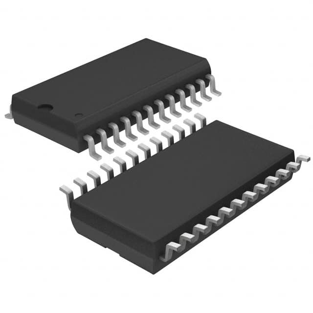
- Part No.:
- CY7B951-SXI
- Manufacturer:
- Cypress Semiconductor Corp
- Category:
- Drivers, Receivers, Transceivers
- Package:
- 24-SOIC (0.295", 7.50mm Width)
- Datasheet:
-
 CY7B951-SXI.pdf
- Description:
- IC TRANSCEIVER FULL 1/1 24SOIC
- Quantity:
- Payment:

- Shipping:

Inventory:1,100
Please send an inquiry. Send us your inquiry, and we will respond immediately.
Product details
Overview
CY7B951-SXI from Cypress Semiconductor is a SONET/SDH and ATM-compatible local area network transceiver IC that recovers clock and data from 51.84-MHz or 155.52-MHz NRZ/NRZI serial streams, provides differential transmit buffering (TOUT±), and delivers ECL 100K-compatible recovered outputs (RCLK±, RSER±, ROUT±). It operates on a single +5V supply in 24-pin SOIC and supports fiber, coaxial, and twisted-pair media.
For engineers reviewing the CY7B951-SXI datasheet, CY7B951-SXI pinout, CY7B951-SXI application, or CY7B951-SXI equivalent, key selection criteria include its dual-rate PLL architecture (51.84/155.52 MHz), ±1% frequency agility, carrier detect–controlled lock behavior, loopback test capability, and integrated power-down modes for RCLK±/RSER±, TCLK±, and output buffers.
Technical Context
The CY7B951-SXI integrates two independent PLLs: a Receive CDR PLL that locks to RIN± using REFCLK×8 as center frequency reference, and a Transmit frequency multiplier PLL that synthesizes TCLK± at exactly 8×REFCLK. Both PLLs are mode-selected via the 3-level MODE pin (VCC/GND/floating) to support STS-1 (51.84 MHz) or STS-3 (155.52 MHz) line rates.
Its receiver includes a transition detector (512-bit-time timeout), Out-of-Lock detection, and Carrier Detect (CD)-gated LFI logic that forces PLL alignment to REFCLK×8 when CD is low. The LOOP pin enables internal TSER±→Receive-PLL routing for full-path functional testing excluding RIN± and TOUT± drivers.
Key Specifications
| Parameter | Value and Actual Design Meaning |
|---|---|
| Data Rates | 51.84 MHz (STS-1) or 155.52 MHz (STS-3); selected by MODE pin level |
| REFCLK Input | 6.48 MHz ±1% (for 51.84 MHz mode) or 19.44 MHz ±1% (for 155.52 MHz mode) |
| Input Sensitivity | RIN± and TSER± accept ≥50 mV differential signals with 2.5 V common-mode range |
| Output Type | ECL 100K-compatible differential outputs (RCLK±, RSER±, ROUT±, TOUT±, TCLK±) |
| Power Supply | +5 V only; operating current <65 mA; power-down reduces per-output current by ~4 mA |
| Frequency Agility | ±1% tolerance on REFCLK ensures stable lock within 1000 ppm of bit rate |
| Loopback Mode | LOOP = LOW routes TSER± to Receive PLL-enables in-system functional validation without external loop |
Pinout & Package
Package: 24-pin SOIC (Small Outline Integrated Circuit), surface-mount, Pb-free option available.
| Pin/Terminal | Circuit Role | Design Meaning |
|---|---|---|
| RIN± | Differential receive input | Directly interfaces low-amplitude PECL data stream; no external buffer needed |
| ROUT± | Differential receive output | Buffered copy of RIN± for equalization or baseline wander compensation |
| RSER± / RCLK± | Differential recovered data/clock | Aligned outputs synchronized to recovered bit timing; compatible with downstream SERDES |
| CD | TTL/ECL carrier detect control | Enables/disables PLL lock to RIN±; forces REFCLK×8 alignment when low |
| LFI | TTL link fault indicator | Combines CD status, transition detection, and OOL to signal LOS/LOF/OOF conditions |
| TSER± | Differential transmit input | Accepts upstream serial data for rebuffering to TOUT±; selectable as CDR source via LOOP |
| TOUT± | Differential transmit output | Drives low-impedance copper media directly; powered down when tied to VCC or floating |
| REFCLK± | Differential/TTL reference clock input | Supports PECL or TTL sources; auto-configures based on voltage level of either pin |
| TCLK± | Differential transmit clock output | Synthesized at 8×REFCLK; powers down entire Transmit PLL when disabled |
| MODE | 3-level frequency mode select | VCC = STS-3 (155.52 MHz), GND = STS-1 (51.84 MHz), floating = test mode |
| LOOP | TTL loopback select | HIGH = RIN± → CDR, LOW = TSER± → CDR for end-to-end path validation |
| VCC / VSS | Power / ground | Single +5 V supply; no separate analog/digital rails required |
Key Features
| Feature | Design Value |
|---|---|
| Dual-rate CDR + frequency multiplier PLL | Single device handles both STS-1 and STS-3 line rates via MODE pin; eliminates need for multiple transceivers |
| Integrated transition and OOL detection | Automatically detects loss of signal integrity (512-bit timeout) and frequency drift (>1000 ppm), driving LFI accordingly |
| Configurable REFCLK interface | Accepts differential PECL or single-ended TTL clock sources without external level-shifting components |
| Per-output power-down capability | Individual disable of RCLK±/RSER±, TCLK±, ROUT±, or TOUT± saves ~4 mA per pair and reduces crosstalk |
| Hardware loopback test mode | LOOP pin enables full CDR functionality test using internal TSER± path-no external loop cable or optical module required |
Applications
| SONET/SDH Line Card | ATM Edge Switch |
|---|---|
Use Scenario: 155.52-MHz OC-3/STM-1 framer interface on telecom line cards handling synchronous optical transport. IC Role / Device Role / Timing Role: Clock and data recovery transceiver providing aligned RCLK±/RSER± to framer ASIC and generating TCLK± for upstream serializer. Use Value: Eliminates external CDR and clock multiplier ICs; MODE = VCC configures for STS-3 operation with 19.44-MHz crystal. | Use Scenario: ATM cell processing in enterprise edge switches connecting legacy T1/E1 to broadband backbones. IC Role / Device Role / Timing Role: Interface between ATM segmentation/reassembly (SAR) controller and physical layer media (twisted pair or fiber). Use Value: ROUT± output used for baseline wander correction on copper links; CD input driven by optical module's LOS signal. |
| Factory Test System | Multi-Rate Protocol Analyzer |
Use Scenario: In-circuit validation of ATM PHY functionality during board manufacturing. IC Role / Device Role / Timing Role: Loopback-enabled CDR verifying SAR-to-PHY data path integrity without optical loopback hardware. Use Value: LOOP = LOW routes TSER± into Receive PLL-confirms CDR lock, RSER±/RCLK± alignment, and LFI behavior under controlled stimulus. | Use Scenario: Field-deployable analyzer capturing and timestamping ATM cells across OC-3 and OC-1 links. IC Role / Device Role / Timing Role: Dual-rate transceiver supporting protocol-agnostic capture at either 51.84 or 155.52 MHz via MODE pin reconfiguration. Use Value: REFCLK flexibility (6.48/19.44 MHz) allows use of same crystal oscillator family across both rates; LFI provides real-time link health flag. |
Equivalent & Alternatives
The following parts are listed as comparable options for similar ATM/SONET transceiver applications.
| Alternative Part | Technical Difference | Application Difference | Selection Advice |
|---|---|---|---|
| PM5345-SUNI | Same pinout and functional compatibility per PMC-Sierra documentation; requires external bias resistors for some PECL interfaces | Designed specifically for SUNI-compliant ATM SAR interfaces; lacks integrated LFI logic and CD-controlled lock override | Select PM5345-SUNI only if existing design uses SUNI register map and external transition detection is already implemented |
| ICS873001AGI | Single-rate (155.52 MHz only); no MODE pin or STS-1 support; higher power (85 mA); different SOIC-28 package | Targeted at fixed-rate OC-3 systems; no loopback or carrier-detect features; requires external REFCLK conditioning | Choose ICS873001AGI only for cost-sensitive OC-3-only deployments where test flexibility and multi-rate support are not required |
Compared with PM5345-SUNI and ICS873001AGI, the CY7B951-SXI uniquely combines dual-rate operation, integrated LFI/CD logic, hardware loopback, and per-output power-down in a 24-pin SOIC-reducing BOM count and enabling field-reconfigurable line cards.
Availability
CY7B951-SXI is available at Aetrix Electronics and suitable for SONET/SDH line cards, ATM edge switches, factory test systems, and multi-rate protocol analyzers requiring stable component supply and long-term lifecycle support.
Supply support for CY7B951-SXI includes scheduled delivery planning, volume procurement assistance, BOM continuity management, traceable sourcing, and lifecycle availability coordination for OEM customers, industrial embedded developers, connected-device designers, and electronics production programs.
Manufacturer
Cypress Semiconductor (now part of Infineon Technologies) designs high-performance mixed-signal ICs for communications, computing, and industrial applications, with emphasis on integration and system-level reliability.
The CY7B951 belongs to Cypress's legacy LAN transceiver product line, engineered specifically for SONET/SDH and ATM physical layer interfacing-prioritizing jitter tolerance, media flexibility, and testability in telecom infrastructure.
FAQ
What is the function of the MODE pin, and how does it affect REFCLK requirements?
The MODE pin is a 3-level input that selects operating frequency: VCC enables 155.52-MHz mode requiring 19.44-MHz ±1% REFCLK; GND enables 51.84-MHz mode requiring 6.48-MHz ±1% REFCLK; floating enables test mode. REFCLK×8 must match the target bit rate within 1000 ppm for reliable lock.
How does the Carrier Detect (CD) pin influence LFI and PLL behavior?
When CD is at ECL HIGH, the Receive PLL tracks RIN± normally and LFI reflects transition and lock status. When CD is at ECL LOW, the PLL locks to REFCLK×8, RSER± holds LOW, and LFI goes LOW-indicating forced alignment. At TTL LOW, only OOL affects LFI.
Can the CY7B951-SXI drive optical modules directly, or is additional circuitry required?
The CY7B951-SXI does not drive lasers or photodiodes directly. Its TOUT± outputs are ECL 100K-compatible and intended for PCB traces, coaxial cable, or twisted pair. Driving optical modules requires external laser driver or limiting amplifier ICs matched to the module's electrical interface.
What happens to the Receive PLL when both RCLK± and RSER± outputs are left unconnected?
Leaving both RCLK± and RSER± unconnected (or tying them to VCC) disables the entire Receive PLL, halting clock/data recovery and reducing current draw. The device retains power to other blocks (e.g., TCLK± generation, LFI logic), but RIN± is ignored until outputs are re-enabled.
CY7B951-SXI Specifications
- Product attributes
- Attribute value
- Manufacturer:
- Cypress Semiconductor Corp
- Series:
- -
- Package/Case:
- 24-SOIC (0.295", 7.50mm Width)
- Packaging:
- Tube
- Product Status:
- Obsolete
- Type:
- Transceiver
- Protocol:
- LAN, ATM
- Number of Drivers/Receivers:
- 1/1
- Duplex:
- Full
- Receiver Hysteresis:
- -
- Data Rate:
- -
- Voltage - Supply:
- 4.5V ~ 5.5V
- Operating Temperature:
- -40°C ~ 85°C
- Grade:
- -
- Qualification:
- -
- Mounting Type:
- Surface Mount
- Supplier Device Package:
- 24-SOIC
CY7B951-SXI FAQ
1.How can I place an order for CY7B951-SXI through Aetrix?
Please submit a Request for Quotation (RFQ) for CY7B951-SXI on Aetrix. Our sales agent will provide a competitive quotation and guide you through the order confirmation once you accept the terms.
2.Are the price and stock information for CY7B951-SXI reliable?
The price and inventory of CY7B951-SXI are updated periodically and may fluctuate due to market conditions. Stock and pricing data are typically refreshed every 24 hours. Quotation validity for CY7B951-SXI is usually 5 days.
3.What payment methods are accepted for CY7B951-SXI?
We accept Wire Transfer, PayPal, Credit Card, Western Union, MoneyGram, and Escrow for CY7B951-SXI transactions.
Note: Certain payment methods may incur a processing fee.
4.How is shipping managed for CY7B951-SXI?
CY7B951-SXI orders can be shipped via leading logistics carriers, including DHL, UPS, FedEx, TNT, or Registered Mail.
Once your CY7B951-SXI order is processed, you will receive an email with the shipment details and tracking number.
Note: Tracking information may take up to 24 hours to appear. Express delivery typically takes 3–5 business days.
5.How can I obtain technical support or documentation for CY7B951-SXI?
For technical support, including CY7B951-SXI datasheets, pinout diagrams, or application guidance, please contact our engineering support team. They can provide detailed documentation and assistance for your CY7B951-SXI requirements.
6.How does Aetrix verify that CY7B951-SXI is sourced from the original manufacturer or authorized distributors?
All CY7B951-SXI products on Aetrix are procured from qualified distributors and authorized channels. Our dedicated quality assurance team conducts strict verification, including traceability checks and, if necessary, third-party testing. This ensures that CY7B951-SXI meets industry standards.
7.What is the process for return or replacement of CY7B951-SXI?
All CY7B951-SXI units undergo pre-shipment inspection (PSI). If there is an issue with CY7B951-SXI, returns or replacements are accepted under the following conditions:
1.Quantity discrepancies, incorrect items, or visible external defects (such as breakage or corrosion), acknowledged by Aetrix.
2.The issue is reported within 90 days of delivery.
3.The CY7B951-SXI part is unused and in its original packaging.
Return procedure for CY7B951-SXI:
1.Submit a request within 90 days.
2.Obtain a Return Material Authorization (RMA) from Aetrix.
CY7B951-SXI Tags

-
ATA6561-GAQW-N
Microchip Technology
-
ATA6561-GBQW-N
Microchip Technology

-
AM26LS32ACDR
Texas Instruments

-
SP485CN-L/TR
MaxLinear, Inc.
-
SP485EN-L/TR
MaxLinear, Inc.
-
SP485EEN-L/TR
MaxLinear, Inc.
-
SP485ECN-L/TR
MaxLinear, Inc.
-
THVD1400DR
Texas Instruments
-
AM26C31IDR
Texas Instruments

-
TLIN1021ADRQ1
Texas Instruments
-
MAX232IDR
Texas Instruments
-
AM26C32IDR
Texas Instruments
Tech Hub

An engineering guide to LED driver operation, constant-current and constant-voltage outputs, linear and switching topologies, dimming, IC selection, calculations, replacement compatibility, and fault c…

Operational amplifier guide covering op amp basics, feedback, ideal vs real op amps, common configurations, buffer circuits, offset, bias current, gain-bandwidth, slew rate, rail-to-rail limits and sel…

Jumper cables guide covering safe connection order, red and black clamp placement, final ground connection, cable gauge, length, clamp quality, copper vs CCA cables, jump starter comparison and battery…

LDO regulator guide covering low dropout voltage, power dissipation, thermal design, PSRR, output noise, capacitor stability, adjustable LDO circuits, LDO vs buck converter and datasheet selection chec…

Conditional Access Module guide covering CAM meaning, CI/CI+ interface, smart card authorization, DVB security workflow, TV and set-top box compatibility, internal electronics, ESD protection, connecto…

Guide to electronic component obsolescence covering EOL risk, PCN/PDN notices, last-time buy planning, replacement options, form-fit-function validation, counterfeit risk and BOM lifecycle management.

18650 battery guide covering lithium-ion cell basics, 3.6V/3.7V voltage, 4.2V charging, mAh and Wh capacity, protected cells, chargers, BMS, series-parallel packs, holders, welding and sourcing checks.…

Hall effect sensor guide covering working principle, linear and digital sensors, Arduino circuits, current sensing, speed detection, automotive applications, A3144 examples, signal filtering and datash…

Product Change Notification guide for electronic components, covering PCN meaning, PCN vs PDN/EOL, common change types, risk levels, form-fit-function review, engineering validation, BOM control, LTB/L…

A practical guide to blend door actuators, covering HVAC function, symptoms, location, AC and heater issues, reset and calibration, replacement cost, electrical diagnosis, compatibility checks, and rep…


