
 My Inquiry
 My Account


Infineon Technologies CY7C025-25JXCT
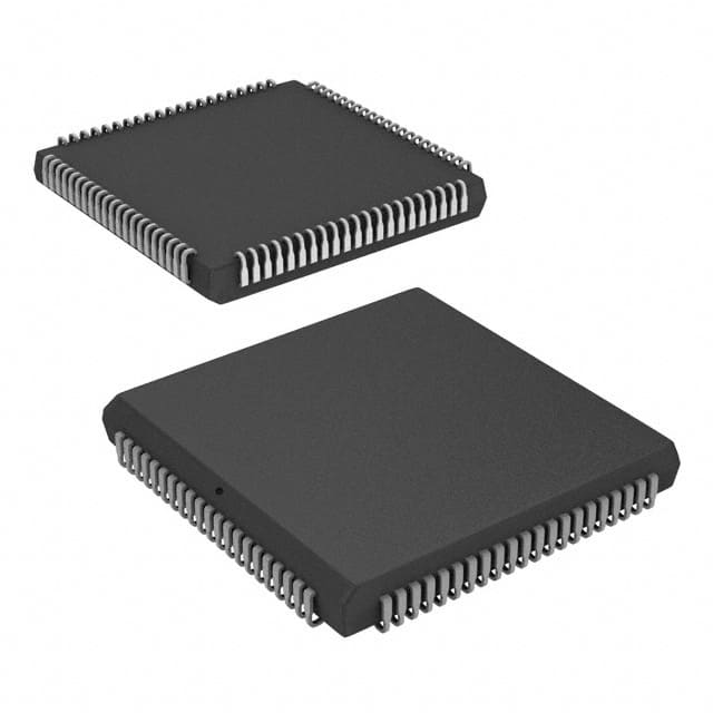
- Part No.:
- CY7C025-25JXCT
- Manufacturer:
- Infineon Technologies
- Category:
- Memory
- Package:
- 84-LCC (J-Lead)
- Datasheet:
-
 CY7C025-25JXCT.pdf
- Description:
- IC SRAM 128KBIT PARALLEL 84PLCC
- Quantity:
- Payment:

- Shipping:

Inventory:1,199
Please send an inquiry. Send us your inquiry, and we will respond immediately.
Product details
Overview
CY7C025-25JXCT from Cypress Semiconductor is an 8K × 16-bit true dual-port static RAM with on-chip arbitration, semaphores, and INT/BUSY flags. It enables simultaneous asynchronous read/write access to shared memory by two independent processors or data paths, supports master/slave expansion to 32-bit bus width, and operates at 25 ns access time with 5 V ±10% supply. Used in interprocessor communication buffers and dual-port video frame stores.
For engineers reviewing the CY7C025-25JXCT datasheet, CY7C025-25JXCT pinout, CY7C025-25JXCT application, or CY7C025-25JXCT equivalent, key selection criteria include dual-port arbitration timing (tPS = 10 ns), semaphore latch count (8), BUSY assertion delay (tBLA = 12 ns), and M/S pin-configurable master/slave operation for scalable memory interfacing.
Technical Context
The CY7C025-25JXCT implements fully asynchronous dual-port architecture with independent CE/R/W/OE controls per port, enabling concurrent access without external synchronization. Its on-chip arbitration logic resolves address-contention events within tPS = 10 ns, and BUSY signals assert deterministically after tBLA = 12 ns (address match) or tBLC = 15 ns (CE low).
Semaphore operation uses eight dedicated latches accessed via SEM pin with A0–A2 addressing; write-to-semaphore requires tSOP = 10 ns OE/SEM deassertion before read, and semaphore value appears at outputs after tSWRD + tDOE = 25 ns. INT flags use upper two memory locations (1FFFH/1FFE H) as mailboxes with automatic reset-on-read behavior.
Key Specifications
| Parameter | Value and Actual Design Meaning |
|---|---|
| Memory Organization | 8K × 16-bit (131,072 bits), supporting independent left/right port access to same address space |
| Access Time | 25 ns maximum - defines minimum cycle time for reliable read/write without wait states |
| Supply Voltage | 5 V ±10% - compatible with standard TTL/CMOS logic rails; no separate I/O voltage required |
| Operating Current | 150 mA typical - determines thermal load and power supply sizing in active dual-port operation |
| Standby Current | 20 mA typical (ISB1) - sets quiescent power draw when one or both ports are disabled via CE |
| Arbitration Timing (tPS) | 10 ns - maximum allowable skew between port address assertions before contention resolution becomes non-deterministic |
| Semaphore Count | 8 independent latches - enables fine-grained resource locking across two processors without memory-mapped overhead |
Pinout & Package
CY7C025-25JXCT is packaged in a 100-pin Pb-free Thin Quad Plastic Flatpack (TQFP) with 0.5 mm pitch, thermally enhanced for industrial temperature operation (–40°C to +85°C). Pin layout supports symmetric left/right port signal routing and M/S configuration for master/slave stacking.
| Pin/Terminal | Circuit Role | Design Meaning |
|---|---|---|
| CEL / CER | Chip Enable (Left/Right) | Independent port activation; drives device into automatic power-down when HIGH |
| R/WL / R/WR | Read/Write Control (Left/Right) | Active-HIGH write enable; asserts write cycle when CE is LOW and OE is HIGH |
| OEL / OER | Output Enable (Left/Right) | Enables bidirectional I/O drivers; must be LOW for read, HIGH for write |
| SEML / SEMR | Semaphore Enable (Left/Right) | Activates semaphore latch access instead of memory array; CE must remain HIGH |
| INTL / INTR | Interrupt Flag (Left/Right) | Open-drain output signaling mailbox write from opposite port; resets on local mailbox read |
| BUSYL / BUSYR | Busy Flag (Left/Right) | In master mode: output indicating arbitration loss; in slave mode: input accepting master's BUSY signal |
| M/S | Master/Slave Select | HIGH configures as master (BUSY pins output); LOW configures as slave (BUSY pins input) |
| UBL / UBR, LBL / LBR | Upper/Lower Byte Select | Enables byte-level write masking: UBL+LBL = full 16-bit write; either alone = 8-bit write |
Key Features
| Feature | Design Value |
|---|---|
| True Dual-Port Memory Cells | Enables deterministic simultaneous reads of identical addresses - eliminates need for external synchronization logic |
| On-Chip Arbitration Logic | Resolves port contention in ≤10 ns (tPS), guaranteeing deterministic BUSY assertion without external glue logic |
| Eight Hardware Semaphores | Dedicated latches accessible via SEM pin - provide atomic resource-locking without consuming main memory space |
| Configurable Master/Slave Mode | M/S pin selects BUSY directionality - enables 32-bit bus expansion using identical parts, no external logic required |
| Mailbox-Based Interrupts | Uses 1FFFH/1FFE H addresses as hardware-managed mailboxes - enables zero-latency inter-processor signaling with auto-reset |
Applications
| Interprocessor Communication Buffer | Dual-Port Video Frame Store |
|---|---|
Use Scenario: Two microcontrollers exchange status, commands, and telemetry data in real time without shared bus contention. IC Role / Device Role / Timing Role: Acts as shared memory hub with hardware arbitration and semaphore-controlled access to prevent race conditions. Use Value: Eliminates software polling loops and external arbitration logic; reduces inter-processor latency to ≤25 ns per memory transaction. | Use Scenario: Graphics controller writes rendered frames while display engine reads previous frame for scanout. IC Role / Device Role / Timing Role: Serves as ping-pong frame buffer with independent left/right port timing - no frame tearing or blanking delays. Use Value: Enables continuous 60 Hz video output with zero-frame-latency rendering using deterministic 25 ns access and BUSY-aware handshaking. |
| Communications Protocol Stack Buffer | Industrial PLC Data Exchange Module |
Use Scenario: Modbus TCP/IP stack processes inbound packets while real-time control layer reads parsed payload. IC Role / Device Role / Timing Role: Provides isolated memory partitions for protocol parsing and control execution, coordinated via INT/mailbox. Use Value: Guarantees deterministic interrupt delivery (<100 ns jitter) and prevents buffer overflow through semaphore-gated packet acceptance. | Use Scenario: PLC CPU and motion controller share I/O state tables and trajectory parameters with strict coherency requirements. IC Role / Device Role / Timing Role: Functions as deterministic shared register file with eight semaphores protecting individual axis control blocks. Use Value: Ensures atomic updates to position setpoints and feedback values - eliminates mid-cycle corruption during high-speed servo cycles. |
Equivalent & Alternatives
The following parts are listed as comparable options for similar dual-port SRAM applications.
| Alternative Part | Technical Difference | Application Difference | Selection Advice |
|---|---|---|---|
| IDT70V25S25PF | 8K × 16-bit, 25 ns, but uses 3.3 V core supply and requires level-shifting for 5 V systems | Lacks integrated M/S pin and hardware mailbox interrupts; relies on external logic for master/slave expansion | Select when migrating to lower-power 3.3 V architecture and external arbitration is acceptable |
| ISSI IS61LV51216-25TQLI | 512K × 16-bit, 25 ns, but single-port only; requires external dual-port controller ASIC | No native semaphore or BUSY logic - increases BOM count and PCB area for equivalent functionality | Select only for high-density storage where dual-port arbitration is handled externally |
Compared with IDT70V25S25PF and IS61LV51216-25TQLI, CY7C025-25JXCT uniquely integrates M/S-configurable arbitration, 8 semaphores, and mailbox interrupts in a 5 V-compatible 100-pin TQFP - reducing system-level complexity and eliminating glue logic for real-time interprocessor coordination.
Availability
CY7C025-25JXCT is available at Aetrix Electronics and suitable for interprocessor communication buffers, dual-port video frame stores, and industrial PLC data exchange modules requiring stable component supply across extended temperature ranges.
Supply support for CY7C025-25JXCT includes scheduled delivery planning, volume procurement assistance, BOM continuity management, traceable sourcing, and lifecycle availability coordination for OEM customers, industrial embedded developers, connected-device designers, and electronics production programs.
Manufacturer
Cypress Semiconductor (now part of Infineon Technologies) designs high-reliability mixed-signal ICs for industrial, automotive, and communications infrastructure applications.
CY7C025 belongs to Cypress's legacy dual-port SRAM product line, engineered specifically for deterministic, low-latency interprocessor memory sharing in real-time embedded systems.
FAQ
What is the function of the M/S pin on CY7C025-25JXCT?
The M/S pin configures the device as master (HIGH) or slave (LOW). In master mode, BUSY pins drive outputs to signal arbitration results; in slave mode, BUSY pins accept inputs from a master device. This enables seamless 32-bit bus expansion using identical CY7C025-25JXCT units without external logic.
How do the semaphore latches operate, and what address range do they use?
Semaphores are eight dedicated latches accessed via SEM pin assertion with A0–A2 selecting the latch (0–7). CE must remain HIGH during SEM activation. Only I/O0 carries the write value; reading returns the latch state on all 16 data lines. No main memory address decoding is involved - semaphores reside outside the 8K × 16 memory map.
Can CY7C025-25JXCT operate reliably at 85°C ambient temperature?
Yes. CY7C025-25JXCT is rated for industrial temperature range (–40°C to +85°C) with 5 V ±10% supply. Electrical characteristics including 25 ns access time, 20 mA standby current, and tPS = 10 ns arbitration timing are guaranteed across this full range per datasheet Rev. *D.
What happens when both ports attempt to write to the same memory location simultaneously?
On-chip arbitration grants access to one port based on tPS timing window (≤10 ns). The losing port asserts its BUSY flag within tBLA = 12 ns (after address match) or tBLC = 15 ns (after CE low). That port's write is blocked until BUSY deasserts - preventing data corruption without external intervention.
CY7C025-25JXCT Specifications
- Product attributes
- Attribute value
- Manufacturer:
- Infineon Technologies
- Series:
- -
- Package/Case:
- 84-LCC (J-Lead)
- Packaging:
- Tape & Reel (TR)
- Product Status:
- Obsolete
- Programmable:
- Not Verified
- Memory Type:
- Volatile
- Memory Format:
- SRAM
- Technology:
- SRAM - Dual Port, Asynchronous
- Memory Size:
- 128Kbit
- Memory Organization:
- 8K x 16
- Memory Interface:
- Parallel
- Clock Frequency:
- -
- Write Cycle Time - Word, Page:
- 25ns
- Access Time:
- 25 ns
- Voltage - Supply:
- 4.5V ~ 5.5V
- Operating Temperature:
- 0°C ~ 70°C (TA)
- Grade:
- -
- Qualification:
- -
- Mounting Type:
- Surface Mount
- Supplier Device Package:
- 84-PLCC (29.31x29.31)
CY7C025-25JXCT FAQ
1.How can I place an order for CY7C025-25JXCT through Aetrix?
Please submit a Request for Quotation (RFQ) for CY7C025-25JXCT on Aetrix. Our sales agent will provide a competitive quotation and guide you through the order confirmation once you accept the terms.
2.Are the price and stock information for CY7C025-25JXCT reliable?
The price and inventory of CY7C025-25JXCT are updated periodically and may fluctuate due to market conditions. Stock and pricing data are typically refreshed every 24 hours. Quotation validity for CY7C025-25JXCT is usually 5 days.
3.What payment methods are accepted for CY7C025-25JXCT?
We accept Wire Transfer, PayPal, Credit Card, Western Union, MoneyGram, and Escrow for CY7C025-25JXCT transactions.
Note: Certain payment methods may incur a processing fee.
4.How is shipping managed for CY7C025-25JXCT?
CY7C025-25JXCT orders can be shipped via leading logistics carriers, including DHL, UPS, FedEx, TNT, or Registered Mail.
Once your CY7C025-25JXCT order is processed, you will receive an email with the shipment details and tracking number.
Note: Tracking information may take up to 24 hours to appear. Express delivery typically takes 3–5 business days.
5.How can I obtain technical support or documentation for CY7C025-25JXCT?
For technical support, including CY7C025-25JXCT datasheets, pinout diagrams, or application guidance, please contact our engineering support team. They can provide detailed documentation and assistance for your CY7C025-25JXCT requirements.
6.How does Aetrix verify that CY7C025-25JXCT is sourced from the original manufacturer or authorized distributors?
All CY7C025-25JXCT products on Aetrix are procured from qualified distributors and authorized channels. Our dedicated quality assurance team conducts strict verification, including traceability checks and, if necessary, third-party testing. This ensures that CY7C025-25JXCT meets industry standards.
7.What is the process for return or replacement of CY7C025-25JXCT?
All CY7C025-25JXCT units undergo pre-shipment inspection (PSI). If there is an issue with CY7C025-25JXCT, returns or replacements are accepted under the following conditions:
1.Quantity discrepancies, incorrect items, or visible external defects (such as breakage or corrosion), acknowledged by Aetrix.
2.The issue is reported within 90 days of delivery.
3.The CY7C025-25JXCT part is unused and in its original packaging.
Return procedure for CY7C025-25JXCT:
1.Submit a request within 90 days.
2.Obtain a Return Material Authorization (RMA) from Aetrix.
CY7C025-25JXCT Tags

-
M24C02-WMN6TP
STMicroelectronics

-
AT24C02C-XHM-T
Microchip Technology

-
AT21CS01-STUM10-T
Microchip Technology

-
AT24C02C-SSHM-T
Microchip Technology

-
24LC01BT-I/OT
Microchip Technology

-
M24C02-FMC6TG
STMicroelectronics
-
AT24CS02-SSHM-T
Microchip Technology

-
93LC46BT-I/OT
Microchip Technology
-
AT24C04C-SSHM-T
Microchip Technology

-
24LC01BT-I/SN
Microchip Technology
-
24AA02UIDT-I/OT
Microchip Technology

-
AT24C08C-STUM-T
Microchip Technology
Tech Hub

An SR latch stores one bit through cross-coupled feedback. This engineering reference covers NOR and NAND implementations, truth tables, forbidden-state recovery, gated operation, switch debouncing, fa…

Latch circuits retain one bit through feedback. This technical reference covers SR and D latches, truth tables, transparency, timing limits, latch-versus-flip-flop behavior, applications and common log…

An engineering guide to LED driver operation, constant-current and constant-voltage outputs, linear and switching topologies, dimming, IC selection, calculations, replacement compatibility, and fault c…

Operational amplifier guide covering op amp basics, feedback, ideal vs real op amps, common configurations, buffer circuits, offset, bias current, gain-bandwidth, slew rate, rail-to-rail limits and sel…

Jumper cables guide covering safe connection order, red and black clamp placement, final ground connection, cable gauge, length, clamp quality, copper vs CCA cables, jump starter comparison and battery…

LDO regulator guide covering low dropout voltage, power dissipation, thermal design, PSRR, output noise, capacitor stability, adjustable LDO circuits, LDO vs buck converter and datasheet selection chec…

Conditional Access Module guide covering CAM meaning, CI/CI+ interface, smart card authorization, DVB security workflow, TV and set-top box compatibility, internal electronics, ESD protection, connecto…

Guide to electronic component obsolescence covering EOL risk, PCN/PDN notices, last-time buy planning, replacement options, form-fit-function validation, counterfeit risk and BOM lifecycle management.

18650 battery guide covering lithium-ion cell basics, 3.6V/3.7V voltage, 4.2V charging, mAh and Wh capacity, protected cells, chargers, BMS, series-parallel packs, holders, welding and sourcing checks.…

Hall effect sensor guide covering working principle, linear and digital sensors, Arduino circuits, current sensing, speed detection, automotive applications, A3144 examples, signal filtering and datash…


