
 My Inquiry
 My Account


Infineon Technologies CY7C1061AV33-10ZXC
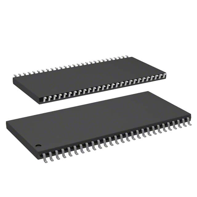
- Part No.:
- CY7C1061AV33-10ZXC
- Manufacturer:
- Infineon Technologies
- Category:
- Memory
- Package:
- 54-TSOP (0.400", 10.16mm Width)
- Datasheet:
-
 CY7C1061AV33-10ZXC.pdf
- Description:
- IC SRAM 16MBIT PAR 54TSOP II
- Quantity:
- Payment:

- Shipping:

Inventory:4,303
Please send an inquiry. Send us your inquiry, and we will respond immediately.
Product details
Overview
CY7C1061AV33-10ZXC from Cypress Semiconductor is a 16-Mbit (1,048,576 × 16) high-speed CMOS static RAM with 10 ns access time, 3.3 V ±0.3 V operation, and automatic CE power-down mode. It supports byte-wide writes via independent BHE/ BLE controls and delivers TTL-compatible I/O for seamless integration into legacy and mixed-voltage memory subsystems, such as industrial PLC data buffers and telecom line card frame storage.
For engineers reviewing the CY7C1061AV33-10ZXC datasheet, CY7C1061AV33-10ZXC pinout, CY7C1061AV33-10ZXC application, or CY7C1061AV33-10ZXC equivalent, key selection criteria include tAA = 10 ns read timing, ISB2 = 50 mA CMOS standby current, dual chip enable (CE1/CE2) logic, 2.0 V data retention voltage, and Pb-free 54-pin TSOP II package compatibility.
Technical Context
This SRAM implements a full synchronous interface with independent byte enables (BHE/BLE) enabling selective upper- or lower-byte writes without external logic. Its dual CE architecture (CE1 active-low, CE2 active-high) allows hierarchical memory banking and easy expansion in multi-chip systems.
The device uses internal voltage regulation to maintain stable core operation during 3.3 V supply transients and supports four distinct operational modes-active read/write, output-disabled, high-impedance deselect, and automatic power-down-governed by precise timing relationships among CE1, CE2, OE, WE, BHE, and BLE.
Key Specifications
| Parameter | Value and Actual Design Meaning |
|---|---|
| tAA | 10 ns maximum address-to-data valid delay - ensures deterministic timing for CPU or FPGA memory controllers running at ≤100 MHz. |
| VCC | 3.3 V ±0.3 V - compatible with standard LVTTL and 3.3 V logic families without level translation. |
| Data Retention Voltage | 2.0 V minimum - enables low-power suspend states while preserving memory contents during brown-out conditions. |
| ISB2 | 50 mA max CMOS standby current - reduces system-level quiescent power in always-on embedded applications. |
| IO Pin Count | 16 bidirectional data lines (IO0–IO15) - supports 16-bit parallel bus architectures without multiplexing. |
| Package | 54-pin TSOP II (Pb-free) - surface-mount footprint optimized for high-density PCB layouts with validated thermal performance up to +70°C ambient. |
| Operating Temperature | 0°C to +70°C (Commercial) - qualified for non-automotive industrial control and networking equipment. |
Pinout & Package
Package: 54-pin Thin Small Outline Package Type II (TSOP II), Pb-free, body size 10.16 mm × 20.00 mm × 1.20 mm, JEDEC MO-141AC compliant.
| Pin/Terminal | Circuit Role | Design Meaning |
|---|---|---|
| A0–A19 | Address Inputs | 20-bit address bus supporting full 1M-word addressing; A0–A19 directly map to physical memory locations. |
| IO0–IO15 | Bidirectional Data I/O | 16-bit parallel data path; direction controlled by WE and OE; high-impedance when deselected or during write cycles. |
| CE1, CE2 | Chip Enable Controls | Complementary enable pair: CE1 = LOW and CE2 = HIGH activates memory; enables hierarchical decoding and bank isolation. |
| WE | Write Enable | Active-low signal initiating write cycles; overlapping CE1/CE2 activation and WE LOW defines write window per truth table. |
| OE | Output Enable | Active-low control for output drivers; must be LOW during reads; high-Z state prevents bus contention. |
| BHE, BLE | Byte High/Low Enables | Independent active-low controls for upper (IO8–IO15) and lower (IO0–IO7) byte lanes - eliminates need for external byte-select logic. |
| VCC, VSS | Power Supply Pins | Three VCC (pins 15, 36, 54) and four VSS (pins 14, 35, 49, 53) provide low-impedance distribution and noise suppression for high-speed operation. |
| NC, DNU | No-Connect / Do-Not-Use | NC pins are unconnected on die; DNU pins (e.g., pin 52) must be tied to VSS or left floating per datasheet to avoid functional disruption. |
Key Features
| Feature | Design Value |
|---|---|
| Automatic CE Power-Down | Reduces ICC to 50 mA (ISB2) when CE2 ≤ 0.3 V and CE1 > VCC – 0.3 V - eliminates need for external sleep controllers in battery-backed systems. |
| Byte-Selectable Write Architecture | Independent BHE/BLE inputs allow simultaneous or staggered upper/lower byte writes - simplifies firmware handling of misaligned data transfers. |
| TTL-Compatible I/O Levels | VIH = 2.0 V min, VOL = 0.4 V max at IOL = 8 mA - ensures interoperability with legacy 5 V-tolerant microcontrollers and FPGAs using 3.3 V I/O banks. |
| 2.0 V Data Retention | Maintains stored data down to 2.0 V VCC - enables graceful low-power suspend/resume in UPS-backed infrastructure and portable instrumentation. |
| Pb-Free TSOP II Packaging | RoHS-compliant 54-pin TSOP II (package code ZXC) - meets IPC/JEDEC standards for reflow soldering and long-term reliability in commercial-grade assemblies. |
Applications
| Industrial PLC Data Buffer | Telecom Line Card Frame Storage |
|---|---|
Use Scenario: Real-time buffering of sensor input streams and control command queues in programmable logic controllers operating in factory-floor environments. IC Role / Device Role / Timing Role: Primary 16-bit parallel SRAM providing deterministic 10 ns read/write access for cyclic executive tasks and interrupt-driven I/O servicing. Use Value: Dual CE architecture enables seamless memory banking across multiple I/O modules; 2.0 V data retention preserves configuration during brief AC mains dips. | Use Scenario: Storing packet header metadata and temporary payload fragments in TDM-based telecom line cards processing E1/T1 traffic. IC Role / Device Role / Timing Role: Low-latency, byte-accessible frame buffer interfaced directly to FPGA-based framer logic with no glue logic required. Use Value: Independent BHE/BLE controls allow efficient 8-bit header updates without disturbing 16-bit payload words; Pb-free TSOP II supports automated SMT assembly. |
| Medical Imaging Subsystem Cache | Test & Measurement Equipment FIFO |
Use Scenario: Temporary storage of digitized waveform segments in portable ultrasound or ECG units requiring fast acquisition and low-power idle states. IC Role / Device Role / Timing Role: High-speed SRAM acting as acquisition-side cache between ADC interface and ARM Cortex-M7 DMA engine. Use Value: 10 ns tAA enables direct coupling to 100 MHz sampling clocks; ISB2 = 50 mA standby current extends battery life during inter-scan intervals. | Use Scenario: First-in-first-out buffering of trigger events and analog capture snapshots in benchtop oscilloscopes and logic analyzers. IC Role / Device Role / Timing Role: Parallel-access memory serving as deep FIFO with byte-granular write capability for mixed-format data streams. Use Value: CE1/CE2-controlled power-down reduces dynamic power during idle periods; TTL-compatible I/O simplifies interface to legacy CPLD-based sequencers. |
Equivalent & Alternatives
The following parts are listed as comparable options for similar high-speed parallel SRAM applications.
| Alternative Part | Technical Difference | Application Difference | Selection Advice |
|---|---|---|---|
| ISSI IS61LV102416-10ML | Same 1M × 16 organization and 10 ns tAA, but uses single CE (active-low) and lacks CE2; IO capacitance 7 pF vs. 8 pF. | Requires redesign of chip select logic; suitable where hierarchical banking is unnecessary. | Select if board space is constrained and CE2 functionality is unused; verify timing margins with reduced IO capacitance. |
| Renesas R1LV1616RSA-10SI | 10 ns tAA, 3.3 V operation, but only single CE and no BHE/BLE - byte masking requires external logic or software overhead. | Higher BOM cost and PCB area due to added discrete logic; limited to full-word writes unless modified. | Prefer only when Renesas supply chain alignment is mandatory; avoid if byte-select efficiency is critical. |
Compared with IS61LV102416-10ML and R1LV1616RSA-10SI, the CY7C1061AV33-10ZXC provides unique dual CE and independent byte enables - reducing external component count and enabling faster partial-word writes in real-time control and telecom applications.
Availability
CY7C1061AV33-10ZXC is available at Aetrix Electronics and suitable for industrial PLC data buffers, telecom line card frame storage, and medical imaging subsystem caches requiring stable component supply and RoHS-compliant packaging.
Supply support for CY7C1061AV33-10ZXC includes scheduled delivery planning, volume procurement assistance, BOM continuity management, traceable sourcing, and lifecycle availability coordination for OEM customers, industrial embedded developers, connected-device designers, and electronics production programs.
Manufacturer
Cypress Semiconductor (now part of Infineon Technologies) designs high-performance memory and programmable solutions for industrial, automotive, and communications markets, with headquarters in San Jose, CA.
The CY7C1061AV33 belongs to Cypress's high-speed parallel SRAM product line, engineered specifically for deterministic, low-latency memory access in real-time embedded systems where bus timing predictability and power-aware standby modes are essential.
FAQ
What is the minimum VCC required to retain data in CY7C1061AV33-10ZXC?
The device guarantees data retention down to 2.0 V VCC, as specified in the DC Electrical Characteristics table. This allows the SRAM to hold memory contents during brown-out conditions or low-power suspend states without external backup power, provided all other pins remain within their defined voltage ranges and no active cycles are initiated.
Can CY7C1061AV33-10ZXC operate with only CE1 asserted, ignoring CE2?
No - the functional truth table requires CE1 = LOW *and* CE2 = HIGH for any active read or write operation. If CE2 is not held HIGH (e.g., left floating or pulled LOW), the device enters power-down mode regardless of CE1 state. CE2 must be actively driven to VIH (≥2.0 V) for normal operation.
Does the 54-pin TSOP II package support reflow soldering per J-STD-020?
Yes - the Pb-free 54-pin TSOP II package (ZXC suffix) complies with JEDEC J-STD-020D moisture sensitivity level 3 and is qualified for standard lead-free reflow profiles with peak temperature up to 260°C. Bake requirements and floor life follow MSL3 guidelines per the Cypress packaging specification document.
How does automatic power-down behave when CE2 is driven to 0.2 V?
When CE2 ≤ 0.3 V and CE1 > VCC – 0.3 V (e.g., CE1 ≥ 3.0 V), the device enters ISB2 power-down mode with typical current draw of 50 mA. At CE2 = 0.2 V, this condition is met, and the SRAM disables outputs, ceases internal refresh, and maintains data integrity at 2.0 V VCC - confirmed by the "Automatic CE Power-down Current - CMOS Inputs" test condition in the datasheet.
CY7C1061AV33-10ZXC Specifications
- Product attributes
- Attribute value
- Manufacturer:
- Infineon Technologies
- Series:
- -
- Package/Case:
- 54-TSOP (0.400", 10.16mm Width)
- Packaging:
- Tray
- Product Status:
- Obsolete
- Programmable:
- Not Verified
- Memory Type:
- Volatile
- Memory Format:
- SRAM
- Technology:
- SRAM - Asynchronous
- Memory Size:
- 16Mbit
- Memory Organization:
- 1M x 16
- Memory Interface:
- Parallel
- Clock Frequency:
- -
- Write Cycle Time - Word, Page:
- 10ns
- Access Time:
- 10 ns
- Voltage - Supply:
- 3V ~ 3.6V
- Operating Temperature:
- 0°C ~ 70°C (TA)
- Grade:
- -
- Qualification:
- -
- Mounting Type:
- Surface Mount
- Supplier Device Package:
- 54-TSOP II
CY7C1061AV33-10ZXC FAQ
1.How can I place an order for CY7C1061AV33-10ZXC through Aetrix?
Please submit a Request for Quotation (RFQ) for CY7C1061AV33-10ZXC on Aetrix. Our sales agent will provide a competitive quotation and guide you through the order confirmation once you accept the terms.
2.Are the price and stock information for CY7C1061AV33-10ZXC reliable?
The price and inventory of CY7C1061AV33-10ZXC are updated periodically and may fluctuate due to market conditions. Stock and pricing data are typically refreshed every 24 hours. Quotation validity for CY7C1061AV33-10ZXC is usually 5 days.
3.What payment methods are accepted for CY7C1061AV33-10ZXC?
We accept Wire Transfer, PayPal, Credit Card, Western Union, MoneyGram, and Escrow for CY7C1061AV33-10ZXC transactions.
Note: Certain payment methods may incur a processing fee.
4.How is shipping managed for CY7C1061AV33-10ZXC?
CY7C1061AV33-10ZXC orders can be shipped via leading logistics carriers, including DHL, UPS, FedEx, TNT, or Registered Mail.
Once your CY7C1061AV33-10ZXC order is processed, you will receive an email with the shipment details and tracking number.
Note: Tracking information may take up to 24 hours to appear. Express delivery typically takes 3–5 business days.
5.How can I obtain technical support or documentation for CY7C1061AV33-10ZXC?
For technical support, including CY7C1061AV33-10ZXC datasheets, pinout diagrams, or application guidance, please contact our engineering support team. They can provide detailed documentation and assistance for your CY7C1061AV33-10ZXC requirements.
6.How does Aetrix verify that CY7C1061AV33-10ZXC is sourced from the original manufacturer or authorized distributors?
All CY7C1061AV33-10ZXC products on Aetrix are procured from qualified distributors and authorized channels. Our dedicated quality assurance team conducts strict verification, including traceability checks and, if necessary, third-party testing. This ensures that CY7C1061AV33-10ZXC meets industry standards.
7.What is the process for return or replacement of CY7C1061AV33-10ZXC?
All CY7C1061AV33-10ZXC units undergo pre-shipment inspection (PSI). If there is an issue with CY7C1061AV33-10ZXC, returns or replacements are accepted under the following conditions:
1.Quantity discrepancies, incorrect items, or visible external defects (such as breakage or corrosion), acknowledged by Aetrix.
2.The issue is reported within 90 days of delivery.
3.The CY7C1061AV33-10ZXC part is unused and in its original packaging.
Return procedure for CY7C1061AV33-10ZXC:
1.Submit a request within 90 days.
2.Obtain a Return Material Authorization (RMA) from Aetrix.
CY7C1061AV33-10ZXC Tags

-
M24C02-WMN6TP
STMicroelectronics

-
AT24C02C-XHM-T
Microchip Technology

-
AT21CS01-STUM10-T
Microchip Technology

-
AT24C02C-SSHM-T
Microchip Technology

-
24LC01BT-I/OT
Microchip Technology

-
M24C02-FMC6TG
STMicroelectronics
-
AT24CS02-SSHM-T
Microchip Technology

-
93LC46BT-I/OT
Microchip Technology
-
AT24C04C-SSHM-T
Microchip Technology

-
24LC01BT-I/SN
Microchip Technology
-
24AA02UIDT-I/OT
Microchip Technology

-
AT24C08C-STUM-T
Microchip Technology
Tech Hub

An SR latch stores one bit through cross-coupled feedback. This engineering reference covers NOR and NAND implementations, truth tables, forbidden-state recovery, gated operation, switch debouncing, fa…

Latch circuits retain one bit through feedback. This technical reference covers SR and D latches, truth tables, transparency, timing limits, latch-versus-flip-flop behavior, applications and common log…

An engineering guide to LED driver operation, constant-current and constant-voltage outputs, linear and switching topologies, dimming, IC selection, calculations, replacement compatibility, and fault c…

Operational amplifier guide covering op amp basics, feedback, ideal vs real op amps, common configurations, buffer circuits, offset, bias current, gain-bandwidth, slew rate, rail-to-rail limits and sel…

Jumper cables guide covering safe connection order, red and black clamp placement, final ground connection, cable gauge, length, clamp quality, copper vs CCA cables, jump starter comparison and battery…

LDO regulator guide covering low dropout voltage, power dissipation, thermal design, PSRR, output noise, capacitor stability, adjustable LDO circuits, LDO vs buck converter and datasheet selection chec…

Conditional Access Module guide covering CAM meaning, CI/CI+ interface, smart card authorization, DVB security workflow, TV and set-top box compatibility, internal electronics, ESD protection, connecto…

Guide to electronic component obsolescence covering EOL risk, PCN/PDN notices, last-time buy planning, replacement options, form-fit-function validation, counterfeit risk and BOM lifecycle management.

18650 battery guide covering lithium-ion cell basics, 3.6V/3.7V voltage, 4.2V charging, mAh and Wh capacity, protected cells, chargers, BMS, series-parallel packs, holders, welding and sourcing checks.…

Hall effect sensor guide covering working principle, linear and digital sensors, Arduino circuits, current sensing, speed detection, automotive applications, A3144 examples, signal filtering and datash…


