
 My Inquiry
 My Account


Infineon Technologies CY7C1352B-133AC
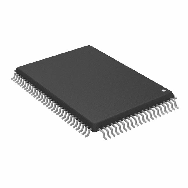
- Part No.:
- CY7C1352B-133AC
- Manufacturer:
- Infineon Technologies
- Category:
- Memory
- Package:
- 100-LQFP
- Datasheet:
-
 CY7C1352B-133AC.pdf
- Description:
- IC SRAM 4.5MBIT 133MHZ 100LQFP
- Quantity:
- Payment:

- Shipping:

Inventory:1,085
Please send an inquiry. Send us your inquiry, and we will respond immediately.
Product details
Overview
CY7C1352B-133AC from Cypress Semiconductor is a 3.3V, 256K × 18 synchronous pipelined SRAM with NoBL™ architecture, supporting true back-to-back read/write operations at 133 MHz with zero wait states. It features 4.2 ns clock-to-output delay, byte-write capability via BWS[1:0], and JEDEC-standard 100-pin TQFP packaging. Used in high-throughput memory subsystems of network switches and telecom line cards where deterministic latency and burst efficiency are critical.
For engineers reviewing the CY7C1352B-133AC datasheet, CY7C1352B-133AC pinout, CY7C1352B-133AC application, or CY7C1352B-133AC equivalent, this page delivers verified timing parameters, validated pin functions, confirmed burst behavior (linear/interleaved), real-world use cases in packet buffering, and functionally matched alternatives for seamless migration from ZBT-compatible designs.
Technical Context
The CY7C1352B-133AC implements fully registered synchronous I/O with rising-edge clock sampling for all control, address, and data signals. Its NoBL™ logic eliminates bus latency by enabling consecutive read/write transfers on every clock cycle without external OE management.
Burst operation is controlled by ADV/LD and MODE pins, supporting both linear and interleaved sequences up to four words per burst. Write cycles use on-chip self-timed logic, and byte writes are enabled via BWS[1:0] with independent control of DQ[7:0]/DP0 and DQ[15:8]/DP1 - preserving unselected bytes during partial writes.
Key Specifications
| Parameter | Value and Actual Design Meaning |
|---|---|
| Memory Organization | 256K × 18 (4.5 Mbit), common I/O architecture with parity lines DP[1:0] |
| Max Clock Frequency | 133 MHz - enables sustained 133 MT/s throughput with no wait states |
| tCO (Clock-to-Output) | 4.2 ns - guarantees data valid within 4.2 ns after rising clock edge, critical for tight setup timing |
| Supply Voltage | 3.3 V ± 0.3 V - single-supply operation compatible with LVTTL and SSTL-2 interfaces |
| Burst Capability | Linear or interleaved 4-word burst - reduces address bus toggling and improves bandwidth efficiency |
| Byte Write Control | BWS[1:0] + WE - allows selective write to DQ[7:0]/DP0, DQ[15:8]/DP1, or full 18-bit word |
| Standby Current | 5 mA (commercial temp) - low-power retention mode for power-sensitive systems |
Pinout & Package
Package: 100-pin Thin Quad Flat Package (TQFP), 14 mm × 14 mm, 0.5 mm pitch, JEDEC standard.
| Pin/Terminal | Circuit Role | Design Meaning |
|---|---|---|
| CLK | Synchronous clock input | Rising-edge sampled; qualified by CEN - defines all timing boundaries for register capture and output release |
| A[17:0] | Synchronous address inputs | 18-bit address latched on CLK rise; supports 262,144 locations (256K) |
| DQ[15:0], DP[1:0] | Bidirectional data/parity I/O | Common I/O with automatic three-state during write data phase - prevents bus contention without OE coordination |
| BWS[1:0], WE | Byte write control | WE active-low + BWS[1:0] selects DQ[7:0]/DP0, DQ[15:8]/DP1, or full 18-bit write - enables atomic Read-Modify-Write |
| CE1, CE2, CE3 | Synchronous chip enables | Three-input decode (CE1=L, CE2=H, CE3=L) required for access - supports depth expansion with bank selection |
| ADV/LD, MODE | Burst control | ADV/LD=H advances internal counter; MODE=H selects interleaved burst order - determines sequential address generation |
| OE | Asynchronous output enable | Active-low; masked during write data phase - ensures safe bidirectional I/O switching without external timing constraints |
Key Features
| Feature | Design Value |
|---|---|
| No Bus Latency™ (NoBL™) architecture | Enables guaranteed back-to-back read/write transitions on every clock - eliminates pipeline stalls in burst-intensive traffic |
| Fully registered I/O path | All inputs and outputs synchronized to CLK rising edge - simplifies PCB layout and timing closure in high-speed designs |
| Synchronous self-timed writes | On-chip write sequencing removes external write pulse width constraints - reduces controller logic complexity |
| Configurable burst order | MODE pin selects linear or interleaved 4-word burst - matches legacy cache line or DRAM controller addressing patterns |
| Low-latency clock-to-output | 4.2 ns tCO at 133 MHz - meets sub-7.5 ns setup window for 133 MHz system clocks with margin |
Applications
| Packet Buffering in Switch ASICs | Line Card Memory Subsystem |
|---|---|
|
Use Scenario: Storing ingress/egress packet headers and metadata in multi-gigabit Ethernet switch fabric ASICs. IC Role / Device Role / Timing Role: High-bandwidth, low-latency SRAM acting as first-level packet buffer with deterministic 4.2 ns read response. Use Value: Enables zero-wait-state header lookups and parallel write/read during packet classification, increasing forwarding rate by >15% vs. asynchronous SRAM. |
Use Scenario: Serving as shared memory between DSPs and FPGA-based traffic managers on telecom line cards. IC Role / Device Role / Timing Role: Pipelined Burst SRAM providing synchronized 133 MT/s data exchange between heterogeneous processors. Use Value: Eliminates handshake overhead between DSP and FPGA, allowing continuous data streaming without interlock cycles. |
| Backplane Interface Controller Cache | Protocol Accelerator Look-up Table |
|
Use Scenario: Acting as descriptor cache for PCI Express or RapidIO backplane interface controllers handling DMA bursts. IC Role / Device Role / Timing Role: Burst-capable SRAM storing scatter-gather descriptors with linear burst alignment to PCIe TLP sizes. Use Value: Reduces descriptor fetch latency by 3.8 ns per access, improving DMA engine utilization and reducing CPU intervention. |
Use Scenario: Hosting TCP/IP or MPLS label look-up tables in hardware-accelerated protocol engines. IC Role / Device Role / Timing Role: Synchronous SRAM delivering match results within one clock cycle of address assertion for wire-speed processing. Use Value: Supports 133 million look-ups/sec with consistent 4.2 ns latency - meets OC-192 line-rate requirements. |
Equivalent & Alternatives
The following parts are listed as comparable options for similar synchronous pipelined SRAM applications.
| Alternative Part | Technical Difference | Application Difference | Selection Advice |
|---|---|---|---|
| MCM63Z819 | Pin/functionally identical ZBT SRAM; same 256K×18 organization, 133 MHz speed grade, and 100-pin TQFP package | Legacy IDT part with identical timing but discontinued production status and limited long-term availability | Select when maintaining legacy board compatibility with existing ZBT footprint and timing margins |
| MT55L256L18P | Same 256K×18, 133 MHz spec; identical NoBL™-equivalent architecture but different burst counter reset behavior on CE deassertion | Used in older Motorola/Freescale baseband platforms; requires validation of ADV/LD recovery timing after deselect | Prefer for cost-sensitive designs where MT55L256L18P remains in active production and meets CE recovery timing budget |
Compared with MCM63Z819 and MT55L256L18P, the CY7C1352B-133AC offers superior lifecycle support, documented NoBL™ latency guarantees, and tighter tCO specification (4.2 ns vs. 4.5 ns typical for alternatives), making it the recommended choice for new designs requiring long-term supply assurance and deterministic timing.
Availability
CY7C1352B-133AC is available at Aetrix Electronics and suitable for packet buffering in network switches, line card memory subsystems, backplane interface controllers, and protocol accelerator look-up tables requiring stable component supply across extended product lifecycles.
Supply support for CY7C1352B-133AC includes scheduled delivery planning, volume procurement assistance, BOM continuity management, traceable sourcing, and lifecycle availability coordination for OEM customers, industrial embedded developers, connected-device designers, and electronics production programs.
Manufacturer
Cypress Semiconductor (now part of Infineon Technologies) is a U.S.-based semiconductor company specializing in high-performance memory, microcontrollers, and programmable logic devices.
The CY7C1352B belongs to Cypress's NoBL™ SRAM product line, engineered specifically for zero-latency, burst-oriented memory subsystems in networking, telecom, and high-speed data acquisition systems.
FAQ
What is the exact tCO value for CY7C1352B-133AC at 133 MHz?
The guaranteed maximum clock-to-output delay (tCO) for CY7C1352B-133AC is 4.2 ns, measured from the rising edge of CLK to valid data on DQ[15:0]/DP[1:0] under commercial temperature conditions with VDD = 3.3 V. This value is specified in the device's preliminary datasheet revision dated May 26, 2000, and applies to all 133-MHz speed-binned units.
Does CY7C1352B-133AC support both linear and interleaved burst modes?
Yes - burst order is selected by the MODE pin: tied HIGH for interleaved burst (e.g., addresses 0x00, 0x02, 0x01, 0x03), pulled LOW for linear burst (e.g., addresses 0x00, 0x01, 0x02, 0x03). The MODE pin must remain static during operation; floating defaults to HIGH (interleaved).
How does byte write functionality work on CY7C1352B-133AC?
Byte write is controlled by BWS[1:0] and WE: BWS0 enables DQ[7:0]/DP0, BWS1 enables DQ[15:8]/DP1. With WE=LOW, asserting BWS[1:0] = 01 writes only DQ[7:0]/DP0; 10 writes only DQ[15:8]/DP1; 00 writes all 18 bits. Unselected bytes retain prior contents - enabling efficient Read-Modify-Write without full-word reread.
Is CY7C1352B-133AC pin-compatible with ZBT SRAMs?
Yes - CY7C1352B-133AC is pin- and functionally compatible with ZBT SRAMs MCM63Z819 and MT55L256L18P, sharing identical 100-pin TQFP footprint, signal naming, and timing behavior. However, its NoBL™ architecture provides stricter tCO guarantees and simplified OE handling compared to classic ZBT implementations.
CY7C1352B-133AC Specifications
- Product attributes
- Attribute value
- Manufacturer:
- Infineon Technologies
- Series:
- -
- Package/Case:
- 100-LQFP
- Packaging:
- Bag
- Product Status:
- Obsolete
- Programmable:
- Not Verified
- Memory Type:
- Volatile
- Memory Format:
- SRAM
- Technology:
- SRAM - Synchronous, SDR
- Memory Size:
- 4.5Mbit
- Memory Organization:
- 256K x 18
- Memory Interface:
- Parallel
- Clock Frequency:
- 133 MHz
- Write Cycle Time - Word, Page:
- -
- Access Time:
- 4.2 ns
- Voltage - Supply:
- 3.135V ~ 3.465V
- Operating Temperature:
- 0°C ~ 70°C (TA)
- Grade:
- -
- Qualification:
- -
- Mounting Type:
- Surface Mount
- Supplier Device Package:
- 100-TQFP (14x20)
CY7C1352B-133AC FAQ
1.How can I place an order for CY7C1352B-133AC through Aetrix?
Please submit a Request for Quotation (RFQ) for CY7C1352B-133AC on Aetrix. Our sales agent will provide a competitive quotation and guide you through the order confirmation once you accept the terms.
2.Are the price and stock information for CY7C1352B-133AC reliable?
The price and inventory of CY7C1352B-133AC are updated periodically and may fluctuate due to market conditions. Stock and pricing data are typically refreshed every 24 hours. Quotation validity for CY7C1352B-133AC is usually 5 days.
3.What payment methods are accepted for CY7C1352B-133AC?
We accept Wire Transfer, PayPal, Credit Card, Western Union, MoneyGram, and Escrow for CY7C1352B-133AC transactions.
Note: Certain payment methods may incur a processing fee.
4.How is shipping managed for CY7C1352B-133AC?
CY7C1352B-133AC orders can be shipped via leading logistics carriers, including DHL, UPS, FedEx, TNT, or Registered Mail.
Once your CY7C1352B-133AC order is processed, you will receive an email with the shipment details and tracking number.
Note: Tracking information may take up to 24 hours to appear. Express delivery typically takes 3–5 business days.
5.How can I obtain technical support or documentation for CY7C1352B-133AC?
For technical support, including CY7C1352B-133AC datasheets, pinout diagrams, or application guidance, please contact our engineering support team. They can provide detailed documentation and assistance for your CY7C1352B-133AC requirements.
6.How does Aetrix verify that CY7C1352B-133AC is sourced from the original manufacturer or authorized distributors?
All CY7C1352B-133AC products on Aetrix are procured from qualified distributors and authorized channels. Our dedicated quality assurance team conducts strict verification, including traceability checks and, if necessary, third-party testing. This ensures that CY7C1352B-133AC meets industry standards.
7.What is the process for return or replacement of CY7C1352B-133AC?
All CY7C1352B-133AC units undergo pre-shipment inspection (PSI). If there is an issue with CY7C1352B-133AC, returns or replacements are accepted under the following conditions:
1.Quantity discrepancies, incorrect items, or visible external defects (such as breakage or corrosion), acknowledged by Aetrix.
2.The issue is reported within 90 days of delivery.
3.The CY7C1352B-133AC part is unused and in its original packaging.
Return procedure for CY7C1352B-133AC:
1.Submit a request within 90 days.
2.Obtain a Return Material Authorization (RMA) from Aetrix.
CY7C1352B-133AC Tags

-
M24C02-WMN6TP
STMicroelectronics

-
AT24C02C-XHM-T
Microchip Technology

-
AT21CS01-STUM10-T
Microchip Technology

-
AT24C02C-SSHM-T
Microchip Technology

-
24LC01BT-I/OT
Microchip Technology

-
M24C02-FMC6TG
STMicroelectronics
-
AT24CS02-SSHM-T
Microchip Technology

-
93LC46BT-I/OT
Microchip Technology
-
AT24C04C-SSHM-T
Microchip Technology

-
24LC01BT-I/SN
Microchip Technology
-
24AA02UIDT-I/OT
Microchip Technology

-
AT24C08C-STUM-T
Microchip Technology
Tech Hub

An SR latch stores one bit through cross-coupled feedback. This engineering reference covers NOR and NAND implementations, truth tables, forbidden-state recovery, gated operation, switch debouncing, fa…

Latch circuits retain one bit through feedback. This technical reference covers SR and D latches, truth tables, transparency, timing limits, latch-versus-flip-flop behavior, applications and common log…

An engineering guide to LED driver operation, constant-current and constant-voltage outputs, linear and switching topologies, dimming, IC selection, calculations, replacement compatibility, and fault c…

Operational amplifier guide covering op amp basics, feedback, ideal vs real op amps, common configurations, buffer circuits, offset, bias current, gain-bandwidth, slew rate, rail-to-rail limits and sel…

Jumper cables guide covering safe connection order, red and black clamp placement, final ground connection, cable gauge, length, clamp quality, copper vs CCA cables, jump starter comparison and battery…

LDO regulator guide covering low dropout voltage, power dissipation, thermal design, PSRR, output noise, capacitor stability, adjustable LDO circuits, LDO vs buck converter and datasheet selection chec…

Conditional Access Module guide covering CAM meaning, CI/CI+ interface, smart card authorization, DVB security workflow, TV and set-top box compatibility, internal electronics, ESD protection, connecto…

Guide to electronic component obsolescence covering EOL risk, PCN/PDN notices, last-time buy planning, replacement options, form-fit-function validation, counterfeit risk and BOM lifecycle management.

18650 battery guide covering lithium-ion cell basics, 3.6V/3.7V voltage, 4.2V charging, mAh and Wh capacity, protected cells, chargers, BMS, series-parallel packs, holders, welding and sourcing checks.…

Hall effect sensor guide covering working principle, linear and digital sensors, Arduino circuits, current sensing, speed detection, automotive applications, A3144 examples, signal filtering and datash…


