
 My Inquiry
 My Account


Infineon Technologies CY7C1360B-166BGC
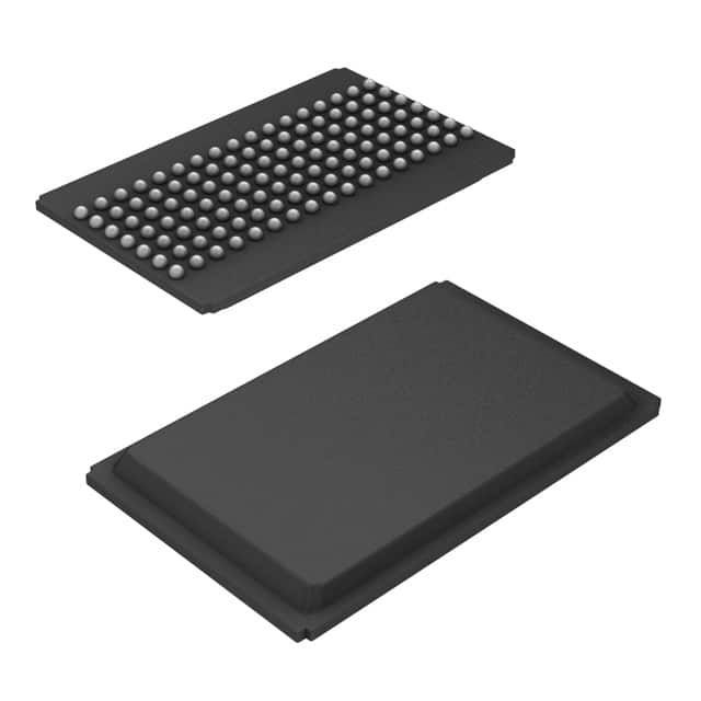
- Part No.:
- CY7C1360B-166BGC
- Manufacturer:
- Infineon Technologies
- Category:
- Memory
- Package:
- 119-BGA
- Datasheet:
-
 CY7C1360B-166BGC.pdf
- Description:
- IC SRAM 9MBIT PARALLEL 119PBGA
- Quantity:
- Payment:

- Shipping:

Inventory:4,417
Please send an inquiry. Send us your inquiry, and we will respond immediately.
Product details
Overview
CY7C1360B-166BGC from Cypress Semiconductor is a 9-Mbit (256K × 36) pipelined synchronous SRAM with registered inputs/outputs, 3.3V core supply, 2.5V/3.3V I/O compatibility, and 166 MHz operation supporting 3-1-1-1 access rate for high-bandwidth memory subsystems in network packet buffers and graphics controllers.
For engineers reviewing the CY7C1360B-166BGC datasheet, CY7C1360B-166BGC pinout, CY7C1360B-166BGC application, or CY7C1360B-166BGC equivalent, key selection criteria include burst mode configuration (interleaved/linear), byte-write control granularity (BWA–BWD + BWE), synchronous self-timed write timing, ZZ sleep mode behavior, and JEDEC-standard 165-ball fBGA package pin mapping.
Technical Context
This SRAM implements a two-bit internal burst counter synchronized to CLK's rising edge, with address latching controlled by ADSP/ADSC strobes and burst advancement triggered by ADV. All synchronous inputs-including addresses, CE1/CE2/CE3, BWX, BWE, GW, and OE-are registered on-chip to enable precise timing control.
It supports synchronous self-timed writes with user-selectable byte-width (1–4 bytes via BWA–BWD), global write (GW active low), and asynchronous output enable (OE) with three-state control. The device operates with separate VDD (3.3V core) and VDDQ (2.5V/3.3V I/O) supplies, and includes IEEE 1149.1 JTAG boundary scan support in fBGA packages.
Key Specifications
| Parameter | Value and Actual Design Meaning |
|---|---|
| Memory Density | 9 Mbit (256K × 36 organization) |
| Max Clock Frequency | 166 MHz - defines maximum sustained burst throughput of 596 MB/s (36-bit bus) |
| Access Time | 3.5 ns - clock-to-output delay under 166 MHz conditions, critical for read-cycle timing closure |
| Core Supply Voltage | 3.3 V ± 0.3 V - powers internal logic and memory array; requires dedicated low-noise regulation |
| I/O Supply Voltage | 2.5 V or 3.3 V - selectable interface voltage matching host processor I/O domain |
| Burst Mode Control | MODE pin strapping - selects Intel Pentium® interleaved or linear burst sequence at power-up |
| Byte Write Capability | Four independent byte lanes (BWA–BWD) + BWE - enables partial-word writes without read-modify-write overhead |
Pinout & Package
Package: 165-ball fine-pitch BGA (fBGA), JEDEC-standard footprint, 1.0 mm ball pitch, RoHS-compliant.
| Pin/Terminal | Circuit Role | Design Meaning |
|---|---|---|
| A0–A[17] | Synchronous Address Input | 18-bit address bus sampled on CLK rising edge when ADSP or ADSC active; A1,A0 load burst counter |
| DQPA–DQPD / DQA–DQD | Synchronous Bidirectional Data I/O | 36-bit data interface with direction controlled by OE; registered input/output paths aligned to CLK |
| CE1, CE2, CE3 | Synchronous Chip Enable | Three-level chip select hierarchy (CE1 active LOW, CE2 active HIGH, CE3 active LOW); enables depth expansion |
| ADSP / ADSC | Address Strobe | Processor (ADSP) or controller (ADSC) address capture signal; only one recognized if both asserted |
| ADV | Burst Advance | Active-LOW signal that increments internal burst counter on CLK rising edge during burst reads/writes |
| BWA–BWD, BWE, GW | Byte Write Control | Four byte-lane enables + byte-write enable (BWE) + global write (GW) for full-word write override |
| OE | Asynchronous Output Enable | Active-LOW; controls I/O direction asynchronously but masks first read cycle after deselect |
| ZZ | Asynchronous Sleep | Active-HIGH; places device in low-power retention mode with data preserved; internal pull-down |
| MODE | Static Burst Configuration | Strap pin: GND = linear burst, VDD/floating = interleaved burst; must remain static during operation |
| VDD / VSS | Core Power / Ground | 3.3V core supply pins (16 locations) and ground (32 locations) - require local decoupling per JEDEC layout rules |
| VDDQ / VSSQ | I/O Power / Ground | Separate 2.5V/3.3V I/O supply (16 pins) and I/O ground (16 pins) - enables mixed-voltage system interfacing |
| TCK/TDI/TDO/TMS | JTAG Boundary Scan | IEEE 1149.1-compliant test interface; TDO available only in fBGA; not present in TQFP |
Key Features
| Feature | Design Value |
|---|---|
| Pipelined Synchronous Interface | Registered address/data/control inputs eliminate external latch timing constraints and simplify high-speed PCB layout |
| 3-1-1-1 Burst Access Rate | Delivers peak bandwidth of 596 MB/s (166 MHz × 36 bits) with minimal latency between consecutive burst words |
| User-Selectable Burst Order | MODE pin configures Intel Pentium®-compatible interleaved or linear burst sequences without firmware intervention |
| Independent Byte Write Control | Four dedicated byte-enable signals (BWA–BWD) plus BWE allow granular 8-bit writes without read-modify-write cycles |
| Dual-Voltage I/O Support | VDDQ configurable for 2.5V or 3.3V operation enables direct interfacing with legacy and modern processors without level shifters |
Applications
| Network Packet Buffering | Graphics Frame Buffer |
|---|---|
Use Scenario: High-throughput line cards buffer incoming/outgoing Ethernet frames before switching or routing decisions. IC Role / Device Role / Timing Role: Primary burst-access SRAM storing packet headers and payloads; operates as synchronous pipeline stage synchronized to switch fabric clock. Use Value: 3-1-1-1 access pattern matches typical packet header + payload burst structure, minimizing idle cycles and maximizing link utilization. | Use Scenario: Embedded GPU subsystem stores frame pixel data and texture maps for real-time rendering pipelines. IC Role / Device Role / Timing Role: Dual-port-capable memory buffer accessed concurrently by display controller and shader units via time-multiplexed bursts. Use Value: Registered I/O and 3.5 ns clock-to-output enable tight timing closure at 166 MHz, reducing display latency and jitter. |
| Industrial Motion Controller Memory | Test Equipment Pattern Memory |
Use Scenario: CNC machine controllers store multi-axis trajectory tables and real-time interpolation coefficients. IC Role / Device Role / Timing Role: Deterministic-latency SRAM providing jitter-free coefficient fetches for servo loop execution at kHz rates. Use Value: ZZ sleep mode reduces standby current to ≤30 mA while preserving position data during idle intervals between motion segments. | Use Scenario: Automated test equipment (ATE) stores high-speed digital stimulus and expected response patterns for IC functional validation. IC Role / Device Role / Timing Role: High-reliability memory bank delivering deterministic 36-bit parallel patterns synchronized to tester clock domain. Use Value: Synchronous self-timed writes ensure accurate pattern loading without external timing calibration, improving test repeatability. |
Equivalent & Alternatives
The following parts are listed as comparable options for similar synchronous pipelined SRAM applications.
| Alternative Part | Technical Difference | Application Difference | Selection Advice |
|---|---|---|---|
| CY7C1362B-166BGC | Same architecture but 512K × 18 organization (9 Mbit); different pinout due to reduced address width and reorganized DQ layout | Preferred where 18-bit data path aligns with DSP or FPGA native bus width; lower pin count simplifies routing | Select when system uses 18-bit-wide memory interfaces and requires identical timing/performance with smaller footprint |
| AS7C3616A-166PCN | 3.3V-only I/O (no 2.5V option); no ZZ sleep mode; lacks JTAG; uses standard 100-pin TQFP instead of fBGA | Suitable for cost-sensitive industrial controllers where sleep mode and advanced test features are unnecessary | Choose for simpler designs requiring drop-in replacement in TQFP-based legacy boards without voltage flexibility or debug requirements |
Compared with CY7C1360B-166BGC, CY7C1362B-166BGC offers identical speed and timing but trades 36-bit width for 18-bit with doubled depth-better for narrow-bus systems-while AS7C3616A-166PCN sacrifices voltage flexibility and debug capability for lower cost and through-hole compatibility.
Availability
CY7C1360B-166BGC is available at Aetrix Electronics and suitable for network packet buffering, graphics frame storage, industrial motion control, and ATE pattern memory applications requiring stable component supply and long-term production continuity.
Supply support for CY7C1360B-166BGC includes scheduled delivery planning, volume procurement assistance, BOM continuity management, traceable sourcing, and lifecycle availability coordination for OEM customers, industrial embedded developers, connected-device designers, and electronics production programs.
Manufacturer
Cypress Semiconductor (now part of Infineon Technologies) is a U.S.-based semiconductor company specializing in high-performance memory, microcontrollers, and programmable logic solutions for industrial, automotive, and communications markets.
The CY7C1360B belongs to Cypress's high-speed synchronous SRAM product line, designed specifically for deterministic-latency, burst-oriented memory subsystems in networking infrastructure and real-time embedded systems.
FAQ
What is the function of the MODE pin on CY7C1360B-166BGC?
The MODE pin is a static configuration input that selects burst order at power-up: tied to GND for linear burst sequence, or to VDD/floating for Intel Pentium®-compatible interleaved burst. It has an internal pull-up resistor and must remain unchanged during operation to avoid burst corruption. This setting determines how the internal two-bit counter increments addresses during burst cycles.
How does the ZZ (Sleep) pin affect power consumption and data retention?
When ZZ is driven HIGH, CY7C1360B-166BGC enters a non-time-critical sleep mode with CMOS standby current limited to ≤30 mA across all speed grades, while retaining all stored data. The pin has an internal pull-down, so it defaults to active-LOW (normal operation) when left unconnected. No clock or refresh is required during sleep, and full functionality resumes within one clock cycle after ZZ returns LOW.
Can CY7C1360B-166BGC operate with 2.5V I/O while using 3.3V core supply?
Yes - CY7C1360B-166BGC supports independent 3.3V core (VDD) and 2.5V or 3.3V I/O (VDDQ) supplies. To use 2.5V I/O, apply 2.5V to all VDDQ pins and ensure OE, CE1, CE2, CE3, ADSP, ADSC, ADV, BWA–BWD, BWE, GW, and CLK signals are referenced to the 2.5V domain. This allows seamless interfacing with 2.5V FPGAs or ASICs without level-shifting circuitry.
What is the role of CE3 in the 165-ball fBGA package?
In the 165-ball fBGA (BGC suffix), CE3 is a fully functional active-LOW chip enable used alongside CE1 (active LOW) and CE2 (active HIGH) to implement three-level depth expansion for building larger memory arrays. Unlike the 2-CE TQFP variant, CE3 is bonded and operational in this package, enabling 3-chip-select configurations for memory systems requiring >9 Mbit capacity via parallel stacking.
CY7C1360B-166BGC Specifications
- Product attributes
- Attribute value
- Manufacturer:
- Infineon Technologies
- Series:
- -
- Package/Case:
- 119-BGA
- Packaging:
- Bag
- Product Status:
- Obsolete
- Programmable:
- Not Verified
- Memory Type:
- Volatile
- Memory Format:
- SRAM
- Technology:
- SRAM - Synchronous, SDR
- Memory Size:
- 9Mbit
- Memory Organization:
- 256K x 36
- Memory Interface:
- Parallel
- Clock Frequency:
- 166 MHz
- Write Cycle Time - Word, Page:
- -
- Access Time:
- 3.5 ns
- Voltage - Supply:
- 3.135V ~ 3.6V
- Operating Temperature:
- 0°C ~ 70°C (TA)
- Grade:
- -
- Qualification:
- -
- Mounting Type:
- Surface Mount
- Supplier Device Package:
- 119-PBGA (14x22)
CY7C1360B-166BGC FAQ
1.How can I place an order for CY7C1360B-166BGC through Aetrix?
Please submit a Request for Quotation (RFQ) for CY7C1360B-166BGC on Aetrix. Our sales agent will provide a competitive quotation and guide you through the order confirmation once you accept the terms.
2.Are the price and stock information for CY7C1360B-166BGC reliable?
The price and inventory of CY7C1360B-166BGC are updated periodically and may fluctuate due to market conditions. Stock and pricing data are typically refreshed every 24 hours. Quotation validity for CY7C1360B-166BGC is usually 5 days.
3.What payment methods are accepted for CY7C1360B-166BGC?
We accept Wire Transfer, PayPal, Credit Card, Western Union, MoneyGram, and Escrow for CY7C1360B-166BGC transactions.
Note: Certain payment methods may incur a processing fee.
4.How is shipping managed for CY7C1360B-166BGC?
CY7C1360B-166BGC orders can be shipped via leading logistics carriers, including DHL, UPS, FedEx, TNT, or Registered Mail.
Once your CY7C1360B-166BGC order is processed, you will receive an email with the shipment details and tracking number.
Note: Tracking information may take up to 24 hours to appear. Express delivery typically takes 3–5 business days.
5.How can I obtain technical support or documentation for CY7C1360B-166BGC?
For technical support, including CY7C1360B-166BGC datasheets, pinout diagrams, or application guidance, please contact our engineering support team. They can provide detailed documentation and assistance for your CY7C1360B-166BGC requirements.
6.How does Aetrix verify that CY7C1360B-166BGC is sourced from the original manufacturer or authorized distributors?
All CY7C1360B-166BGC products on Aetrix are procured from qualified distributors and authorized channels. Our dedicated quality assurance team conducts strict verification, including traceability checks and, if necessary, third-party testing. This ensures that CY7C1360B-166BGC meets industry standards.
7.What is the process for return or replacement of CY7C1360B-166BGC?
All CY7C1360B-166BGC units undergo pre-shipment inspection (PSI). If there is an issue with CY7C1360B-166BGC, returns or replacements are accepted under the following conditions:
1.Quantity discrepancies, incorrect items, or visible external defects (such as breakage or corrosion), acknowledged by Aetrix.
2.The issue is reported within 90 days of delivery.
3.The CY7C1360B-166BGC part is unused and in its original packaging.
Return procedure for CY7C1360B-166BGC:
1.Submit a request within 90 days.
2.Obtain a Return Material Authorization (RMA) from Aetrix.
CY7C1360B-166BGC Tags

-
M24C02-WMN6TP
STMicroelectronics

-
AT24C02C-XHM-T
Microchip Technology

-
AT21CS01-STUM10-T
Microchip Technology

-
AT24C02C-SSHM-T
Microchip Technology

-
24LC01BT-I/OT
Microchip Technology

-
M24C02-FMC6TG
STMicroelectronics
-
AT24CS02-SSHM-T
Microchip Technology

-
93LC46BT-I/OT
Microchip Technology
-
AT24C04C-SSHM-T
Microchip Technology

-
24LC01BT-I/SN
Microchip Technology
-
24AA02UIDT-I/OT
Microchip Technology

-
AT24C08C-STUM-T
Microchip Technology
Tech Hub
A technical comparison of level-sensitive latches and edge-triggered flip-flops, covering timing windows, setup and hold limits, master–slave operation, time borrowing, race-through, HDL inference and…
A D latch stores one bit while Enable controls when data can pass. This reference covers gate-level operation, truth tables, transparency, setup and hold timing, LE versus OE, common ICs and practical …

An SR latch stores one bit through cross-coupled feedback. This engineering reference covers NOR and NAND implementations, truth tables, forbidden-state recovery, gated operation, switch debouncing, fa…

Latch circuits retain one bit through feedback. This technical reference covers SR and D latches, truth tables, transparency, timing limits, latch-versus-flip-flop behavior, applications and common log…

An engineering guide to LED driver operation, constant-current and constant-voltage outputs, linear and switching topologies, dimming, IC selection, calculations, replacement compatibility, and fault c…

Operational amplifier guide covering op amp basics, feedback, ideal vs real op amps, common configurations, buffer circuits, offset, bias current, gain-bandwidth, slew rate, rail-to-rail limits and sel…

Jumper cables guide covering safe connection order, red and black clamp placement, final ground connection, cable gauge, length, clamp quality, copper vs CCA cables, jump starter comparison and battery…

LDO regulator guide covering low dropout voltage, power dissipation, thermal design, PSRR, output noise, capacitor stability, adjustable LDO circuits, LDO vs buck converter and datasheet selection chec…

Conditional Access Module guide covering CAM meaning, CI/CI+ interface, smart card authorization, DVB security workflow, TV and set-top box compatibility, internal electronics, ESD protection, connecto…

Guide to electronic component obsolescence covering EOL risk, PCN/PDN notices, last-time buy planning, replacement options, form-fit-function validation, counterfeit risk and BOM lifecycle management.


