
 My Inquiry
 My Account


Infineon Technologies CY7C341B-25JC
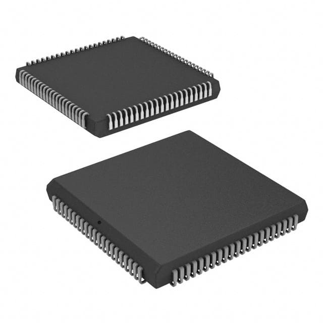
- Part No.:
- CY7C341B-25JC
- Manufacturer:
- Infineon Technologies
- Category:
- PLDs (Programmable Logic Device)
- Package:
- 84-LCC (J-Lead)
- Datasheet:
-
 CY7C341B-25JC.pdf
- Description:
- IC PLD 192MC 25NS 84PLCC
- Quantity:
- Payment:

- Shipping:

Inventory:2,873
Please send an inquiry. Send us your inquiry, and we will respond immediately.
Product details
Overview
CY7C341B-25JC from Cypress Semiconductor is a 192-macrocell Erasable Programmable Logic Device (EPLD) based on MAX® architecture, implementing user-configurable combinational and registered logic functions. It features 12 Logic Array Blocks (LABs), 8 dedicated inputs (including one system clock input), 64 bidirectional I/O pins, 384 expander product terms, and operates at 5V with 25 ns maximum access time in commercial temperature range (0°C to +70°C).
For engineers reviewing the CY7C341B-25JC datasheet, CY7C341B-25JC pinout, CY7C341B-25JC application, or CY7C341B-25JC equivalent, key selection considerations include macrocell count, LAB-level expander term allocation, fixed-delay programmable interconnect array (PIA), I/O configuration flexibility, and EPROM-based nonvolatile configuration security.
Technical Context
The CY7C341B-25JC implements a fully user-programmable MAX® architecture with 12 LABs-each containing 16 macrocells, 32 expander product terms, and dedicated I/O blocks. All macrocell feedback paths route through the PIA, enabling full inter-LAB signal routing without timing skew.
Its programmable interconnect array delivers fixed delay (14–20 ns), eliminating variable routing-induced skews common in gate arrays. The device supports both synchronous and asynchronous clocking modes, with separate timing parameters for dedicated inputs (tPD1 = 25 ns), I/O inputs (tPD2 = 40 ns), and register-to-output (tCO1 = 14 ns).
Key Specifications
| Parameter | Value and Actual Design Meaning |
|---|---|
| Macrocell Count | 192 macrocells distributed across 12 LABs (16 per LAB); enables complex state-machine and glue-logic replacement. |
| Logic Array Blocks | 12 LABs with 32 shared expander product terms each; increases effective logic density without increasing macrocell complexity. |
| Maximum Access Time | 25 ns (7C341B-25 speed grade); defines worst-case propagation delay from input to combinatorial output under commercial conditions. |
| I/O Pins | 64 bidirectional I/O pins, individually configurable as input, output, or tristate; supports mixed-signal board-level integration. |
| Dedicated Inputs | 8 dedicated inputs including one designated system clock pin; provides low-skew global control signals independent of I/O routing. |
| Supply Voltage | 5.0 V ±5% (commercial range); requires decoupling ≥0.2 µF per VCC pin using monolithic ceramic capacitors. |
| Operating Temperature | 0°C to +70°C (commercial grade); validated for stable operation across full range with guaranteed AC/DC specs. |
| Configuration Technology | CMOS EPROM cells; retains logic configuration without power; design security bit prevents readback of programmed data. |
Pinout & Package
The CY7C341B-25JC is packaged in an 84-pin Plastic Leaded Chip Carrier (PLCC), J83 package type, with gull-wing leads and body size 29.31 mm × 29.31 mm. Pin 1 is marked by a corner notch; pin numbering proceeds counterclockwise.
| Pin/Terminal | Circuit Role | Design Meaning |
|---|---|---|
| 1 (A6) | INPUT/CLK | Primary system clock input; drives global synchronous logic paths with tSU = 15 ns setup requirement. |
| 2 (A5), 41–43, 44, 46–49, 50–53, 54–56, 57–59, 62–65, 67–74, 75–79, 80–82 | I/O | Bidirectional pins; configurable per macrocell assignment; support tristate control via tZX/tXZ delays (10–13 ns). |
| 3, 24, 45, 66 (B5, G2, K7, E10) | INPUT | Dedicated general-purpose inputs; bypass I/O buffer path for lower latency (tPD1 = 25 ns vs. tPD2 = 40 ns). |
| 4–16, 17–23, 25–29, 30–35, 36–40, 60–61, 81–82 | INPUT | Additional dedicated inputs; used for control signals, address lines, or asynchronous reset/preset paths. |
| VCC (pins 18, 19, 39, 40, 60, 61, 81, 82) | Power Supply | Eight VCC pins require local 0.2 µF ceramic decoupling; ensures stable voltage during high-speed macrocell switching. |
| GND (pins 20, 21, 22, 34, 35, 37, 38, 42, 43, 44, 45, 46, 47, 48, 58, 59, 62, 63, 64, 65, 67, 68, 69, 70, 71, 72, 73, 74, 83, 84) | Ground | 30 GND pins provide low-inductance return paths; mandatory direct connection between adjacent VCC/GND pairs at package edge. |
Key Features
| Feature | Design Value |
|---|---|
| Programmable Interconnect Array (PIA) | Fixed 14–20 ns delay routing; eliminates signal skew across LABs and enables single-pass timing closure. |
| LAB-Level Expander Product Terms | 32 expanders per LAB shared among 16 macrocells; extends logic capability without increasing macrocell product-term count. |
| Design Security Bit | EPROM-level read-protection; prevents unauthorized extraction of programmed logic configuration after programming. |
| Nonvolatile EPROM Configuration | Retains logic design indefinitely without external memory or configuration PROM; supports instant-on operation. |
| Multiple Clock Domains | Supports dedicated synchronous clock (tCO1 = 14 ns), asynchronous clock (tACO1 = 25 ns), and global clock (tCNT = 20 ns min period). |
| Testability | On-board logic test circuitry validates AC/DC functionality post-encapsulation-even in non-windowed PLCC packages. |
Applications
| Industrial Control Logic | Legacy TTL Replacement |
|---|---|
|
Use Scenario: Replacing discrete 7400-series logic in PLC backplane interface modules requiring deterministic timing and field-upgradable logic. IC Role / Device Role / Timing Role: Configurable glue logic implementing address decoding, bus arbitration, and status encoding with fixed PIA delay. Use Value: Reduces 75+ TTL devices into single CY7C341B-25JC, cutting PCB area by >60% and eliminating inter-device skew. |
Use Scenario: Consolidating combinatorial and registered logic in aging telecom line-card designs where board space and reliability are critical. IC Role / Device Role / Timing Role: Standalone logic replacement with 25 ns access time meeting legacy timing budgets for control-plane signaling. Use Value: Eliminates solder joint fatigue from multiple ICs; EPROM retention ensures unchanged behavior over 10+ year deployments. |
| Embedded System Boot Controller | Test Equipment Pattern Generator |
|
Use Scenario: Managing power sequencing, FPGA configuration handoff, and watchdog supervision in medical imaging subsystems. IC Role / Device Role / Timing Role: Nonvolatile state machine coordinating multi-rail power-up with precise tSU/tH timing relative to system clock. Use Value: Removes external microcontroller dependency; design security prevents tampering with boot integrity logic. |
Use Scenario: Generating synchronized stimulus waveforms for ATE systems requiring sub-25 ns edge alignment across 64 channels. IC Role / Device Role / Timing Role: High-fanout registered pattern generator using LAB-local registers and PIA-routed clocks. Use Value: Achieves 62.5 MHz toggle frequency (fMAX) with deterministic skew <1 ns between outputs due to fixed PIA delay. |
Equivalent & Alternatives
The following parts are listed as comparable options for similar EPLD-based logic replacement applications.
| Alternative Part | Technical Difference | Application Difference | Selection Advice |
|---|---|---|---|
| CY7C342B-25JC | 256 macrocells, 16 LABs, same 84-pin PLCC; higher density but identical timing architecture and PIA structure. | Required when logic function exceeds 192 macrocells; no change to board layout or timing analysis methodology. | Select when design scales beyond 192 macrocells but must retain identical pinout, voltage, and thermal profile. |
| ATF1504AS-25JC | 256 macrocells, Flash-based configuration (non-UV-erasable), 3.3V core; different programming model and voltage domain. | Suitable for new 3.3V designs requiring reprogrammability in-system; incompatible with 5V-only legacy boards. | Choose only for green-field 3.3V systems; not drop-in compatible due to voltage, programming interface, and timing model differences. |
Compared with CY7C341B-25JC, CY7C342B-25JC offers scalable density within identical mechanical and electrical constraints, while ATF1504AS-25JC shifts to Flash technology and 3.3V operation-requiring full redesign of power delivery, I/O interfacing, and programming infrastructure.
Availability
CY7C341B-25JC is available at Aetrix Electronics and suitable for industrial control logic, legacy TTL replacement, embedded boot controller, and ATE pattern generation requiring stable component supply and long-lifecycle support.
Supply support for CY7C341B-25JC includes scheduled delivery planning, volume procurement assistance, BOM continuity management, traceable sourcing, and lifecycle availability coordination for OEM customers, industrial embedded developers, connected-device designers, and electronics production programs.
Manufacturer
Cypress Semiconductor (now part of Infineon Technologies) is a U.S.-based semiconductor company specializing in programmable logic, memory, and mixed-signal solutions for industrial, automotive, and communications markets.
The CY7C341B belongs to the MAX® EPLD product line, designed specifically for high-density, nonvolatile, pin-compatible logic consolidation in cost-sensitive, long-lifecycle applications where field reprogrammability is not required.
FAQ
Is CY7C341B-25JC UV-erasable, and what equipment is needed?
Yes, CY7C341B-25JC uses UV-erasable EPROM cells housed in a windowed ceramic package variant (e.g., -25HC), but the -25JC variant is plastic-leaded (PLCC) and non-UV-erasable. Erasure requires exposure to 253.7 nm UV light at ≥12,000 µW/cm² for 20–30 minutes. The -25JC must be programmed once and retained permanently; it cannot be erased in-circuit or with standard UV erasers.
What is the maximum number of I/O pins usable simultaneously in a design?
All 64 I/O pins can be used concurrently, but actual utilization depends on LAB resource allocation: LABs A/F/G/L allocate 8 I/O-connected macrocells each, while LABs B–E/H–K allocate only 4. Total I/O pin count remains 64, but simultaneous registered I/O drive capability is constrained by macrocell-to-I/O mapping-not pin count alone.
Does CY7C341B-25JC support hot-swap or live-insertion?
No. The device lacks hot-swap protection circuitry. Power sequencing must follow strict ramp requirements: VCC must stabilize before applying any input signals, and all inputs must remain within GND < VIN < VCC during power transitions. Violation risks latch-up or permanent damage per Absolute Maximum Ratings (−2.0 V to +7.0 V transient limit).
How does the programmable interconnect array (PIA) affect timing predictability?
The PIA guarantees fixed 14–20 ns routing delay regardless of signal path length or fanout-unlike FPGA routing fabrics. This eliminates timing skew between parallel logic paths, enabling deterministic setup/hold timing across all LABs and simplifying static timing analysis for pipeline-critical applications like ATE waveform generation.
CY7C341B-25JC Specifications
- Product attributes
- Attribute value
- Manufacturer:
- Infineon Technologies
- Series:
- -
- Package/Case:
- 84-LCC (J-Lead)
- Packaging:
- Tube
- Product Status:
- Obsolete
- Programmable:
- Not Verified
- Programmable Type:
- EPLD
- Number of Macrocells:
- 192
- Voltage - Input:
- 5V
- Speed:
- 25 ns
- Mounting Type:
- Surface Mount
- Supplier Device Package:
- 84-PLCC (29.31x29.31)
CY7C341B-25JC FAQ
1.How can I place an order for CY7C341B-25JC through Aetrix?
Please submit a Request for Quotation (RFQ) for CY7C341B-25JC on Aetrix. Our sales agent will provide a competitive quotation and guide you through the order confirmation once you accept the terms.
2.Are the price and stock information for CY7C341B-25JC reliable?
The price and inventory of CY7C341B-25JC are updated periodically and may fluctuate due to market conditions. Stock and pricing data are typically refreshed every 24 hours. Quotation validity for CY7C341B-25JC is usually 5 days.
3.What payment methods are accepted for CY7C341B-25JC?
We accept Wire Transfer, PayPal, Credit Card, Western Union, MoneyGram, and Escrow for CY7C341B-25JC transactions.
Note: Certain payment methods may incur a processing fee.
4.How is shipping managed for CY7C341B-25JC?
CY7C341B-25JC orders can be shipped via leading logistics carriers, including DHL, UPS, FedEx, TNT, or Registered Mail.
Once your CY7C341B-25JC order is processed, you will receive an email with the shipment details and tracking number.
Note: Tracking information may take up to 24 hours to appear. Express delivery typically takes 3–5 business days.
5.How can I obtain technical support or documentation for CY7C341B-25JC?
For technical support, including CY7C341B-25JC datasheets, pinout diagrams, or application guidance, please contact our engineering support team. They can provide detailed documentation and assistance for your CY7C341B-25JC requirements.
6.How does Aetrix verify that CY7C341B-25JC is sourced from the original manufacturer or authorized distributors?
All CY7C341B-25JC products on Aetrix are procured from qualified distributors and authorized channels. Our dedicated quality assurance team conducts strict verification, including traceability checks and, if necessary, third-party testing. This ensures that CY7C341B-25JC meets industry standards.
7.What is the process for return or replacement of CY7C341B-25JC?
All CY7C341B-25JC units undergo pre-shipment inspection (PSI). If there is an issue with CY7C341B-25JC, returns or replacements are accepted under the following conditions:
1.Quantity discrepancies, incorrect items, or visible external defects (such as breakage or corrosion), acknowledged by Aetrix.
2.The issue is reported within 90 days of delivery.
3.The CY7C341B-25JC part is unused and in its original packaging.
Return procedure for CY7C341B-25JC:
1.Submit a request within 90 days.
2.Obtain a Return Material Authorization (RMA) from Aetrix.
CY7C341B-25JC Tags
-
ATF16V8B-15PU
Microchip Technology
-
ATF16V8B-15JU
Microchip Technology
-
ATF16V8BQL-15PU
Microchip Technology
-
ATF22V10C-15PU
Microchip Technology
.jpg)
-
ATF22V10C-15JU
Microchip Technology
-
ATF22V10C-10JU
Microchip Technology
-
ATF22V10B-15GM/883
Microchip Technology

-
ATF16V8B-15SU
Microchip Technology
-
ATF16V8BQL-15SU
Microchip Technology
-
ATF16V8BQL-15JU
Microchip Technology
-
ATF16V8B-10JU
Microchip Technology
-
ATF16V8BQL-15XU
Microchip Technology
Tech Hub

Operational amplifier guide covering op amp basics, feedback, ideal vs real op amps, common configurations, buffer circuits, offset, bias current, gain-bandwidth, slew rate, rail-to-rail limits and sel…

Jumper cables guide covering safe connection order, red and black clamp placement, final ground connection, cable gauge, length, clamp quality, copper vs CCA cables, jump starter comparison and battery…

LDO regulator guide covering low dropout voltage, power dissipation, thermal design, PSRR, output noise, capacitor stability, adjustable LDO circuits, LDO vs buck converter and datasheet selection chec…

Conditional Access Module guide covering CAM meaning, CI/CI+ interface, smart card authorization, DVB security workflow, TV and set-top box compatibility, internal electronics, ESD protection, connecto…

Guide to electronic component obsolescence covering EOL risk, PCN/PDN notices, last-time buy planning, replacement options, form-fit-function validation, counterfeit risk and BOM lifecycle management.

18650 battery guide covering lithium-ion cell basics, 3.6V/3.7V voltage, 4.2V charging, mAh and Wh capacity, protected cells, chargers, BMS, series-parallel packs, holders, welding and sourcing checks.…

Hall effect sensor guide covering working principle, linear and digital sensors, Arduino circuits, current sensing, speed detection, automotive applications, A3144 examples, signal filtering and datash…

Product Change Notification guide for electronic components, covering PCN meaning, PCN vs PDN/EOL, common change types, risk levels, form-fit-function review, engineering validation, BOM control, LTB/L…

A practical guide to blend door actuators, covering HVAC function, symptoms, location, AC and heater issues, reset and calibration, replacement cost, electrical diagnosis, compatibility checks, and rep…

Engineering guide to Raspberry Pi alternatives, covering chip-level differences, Orange Pi, ROCK, Jetson, Banana Pi, NanoPi, Compute Module, Pico, GPIO, camera, HAT compatibility, and replacement risks…


