
 My Inquiry
 My Account


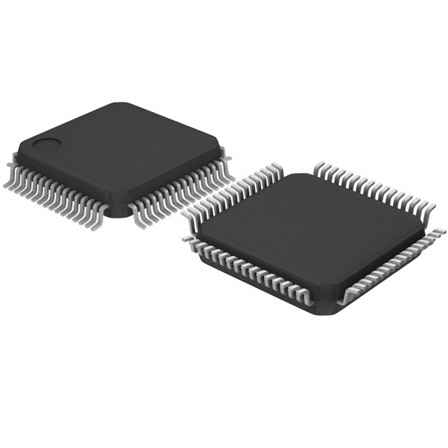
Infineon Technologies CY7C4225-15AXC
- Part No.:
- CY7C4225-15AXC
- Manufacturer:
- Infineon Technologies
- Category:
- FIFOs Memory
- Package:
- 64-LQFP
- Datasheet:
-
 CY7C4225-15AXC.pdf
- Description:
- IC FIFO SYNC 1KX18 10NS 64TQFP
- Quantity:
- Payment:

- Shipping:

Inventory:2,072
Please send an inquiry. Send us your inquiry, and we will respond immediately.
Product details
Overview
CY7C4225-15AXC from Cypress Semiconductor is a 1K × 18-bit synchronous FIFO memory with TTL-compatible interfaces, 10 ns read/write cycle time at 100 MHz, 45 mA operating current, and programmable Almost Empty/Almost Full flags. It serves as a high-speed data buffer in asynchronous communication bridges between processors, FPGAs, or ADC/DAC subsystems requiring deterministic latency and depth expansion capability.
For engineers reviewing the CY7C4225-15AXC datasheet, CY7C4225-15AXC pinout, CY7C4225-15AXC application, or CY7C4225-15AXC equivalent, key selection criteria include its dual-clock asynchronous operation, 18-bit bus width, retransmit function for packet recovery, and support for both width and depth cascading in industrial control and telecom interface designs.
Technical Context
The CY7C4225-15AXC implements a dual-port SRAM array (1024 × 18 bits) controlled by independent WCLK and RCLK inputs, enabling true simultaneous read/write operations without arbitration. Its flag logic includes synchronous EF (tied to RCLK) and FF (tied to WCLK), plus programmable PAE/PAF whose synchronization mode depends on VCC/SMODE pin state.
Depth expansion uses WXI/WXO and RXI/RXO pins with FL pin sequencing across daisy-chained devices; width expansion connects multiple units in parallel using shared clocks and enables while splitting the 18-bit bus. Retransmit (RT) resets the read pointer to enable repeat transmission of buffered packets without host intervention.
Key Specifications
| Parameter | Value and Actual Design Meaning |
|---|---|
| Density | 1024 × 18 bits - provides 18-bit-wide buffering for up to 1024 words, suitable for burst-mode data streams in video or packetized protocols. |
| Max Clock Frequency | 100 MHz - supports 10 ns read/write cycle time, enabling real-time interfacing with high-speed microcontrollers and FPGAs. |
| Operating Current | 45 mA @ 20 MHz - low power consumption allows integration into thermally constrained embedded systems without forced cooling. |
| Status Flags | EF, FF, HF, PAE, PAF - five decoded flags deliver precise FIFO state awareness; HF shares WXO pin and remains valid in standalone/width-expansion modes. |
| Programmable Offsets | 12-bit PAE/PAF registers - allow user-defined trigger points (default: 127 words from Empty/Full) for early flow control signaling in custom protocol stacks. |
| Retransmit Function | FL/RT pin dual-mode - enables packet replay by resetting read pointer to first location, critical for loss-tolerant serial or SPI-based link layers. |
| Expansion Support | Width and depth expansion - WXO/HF, RXO, WXI, RXI pins permit scalable buffering beyond 1K depth or wider than 18-bit buses via cascading. |
Pinout & Package
Package: 64-pin TQFP (10 mm × 10 mm, 0.5 mm pitch) - compact surface-mount footprint compatible with high-density PCB layouts and automated assembly.
| Pin/Terminal | Circuit Role | Design Meaning |
|---|---|---|
| D0–D17 | Input Data Bus | 18-bit parallel write data path; accepts TTL-level signals synchronized to WCLK rising edge when WEN is active low. |
| Q0–Q17 | Output Data Bus | 18-bit parallel read data path; three-state controlled by OE; outputs valid after tOE delay from RCLK edge when REN is active low. |
| WEN, REN | Enable Controls | Independent write/read gate signals - must meet tENS setup before respective clock edges to ensure reliable data capture or output. |
| WCLK, RCLK | Clock Inputs | Free-running TTL clocks - may be tied together for single-clock operation or run independently for full asynchronous buffering. |
| EF, FF, PAE, PAF, WXO/HF | Status Outputs | Synchronous flags updated on RCLK (EF, PAE) or WCLK (FF, PAF); WXO/HF serves as Half Full flag or depth-expansion signal depending on configuration. |
| FL/RT | Mode Control | Dual-function pin: FL selects first device in cascade chain (tied to VSS); RT enables retransmit in standalone mode via pulse. |
| VCC/SMODE | Flag Synchronization Mode | Tie to VSS for synchronous PAE/PAF (PAE→RCLK, PAF→WCLK); tie to VCC for asynchronous operation - affects timing predictability in safety-critical reads. |
Key Features
| Feature | Design Value |
|---|---|
| Independent Read/Write Clock Domains | Enables seamless bridging between mismatched clock domains (e.g., 50 MHz FPGA fabric ↔ 80 MHz DSP core) without handshake logic. |
| Programmable Almost Full/Empty Thresholds | 12-bit offset registers allow fine-grained flow control tuning - avoids overflow/underflow in variable-rate streaming applications like audio sample rate conversion. |
| Retransmit Capability | Hardware-accelerated packet replay eliminates software polling overhead and guarantees deterministic recovery latency in UART/SPI-based telemetry links. |
| Center-Power/Ground Layout | Reduces switching noise coupling between I/O and core logic - improves signal integrity in mixed-signal systems with sensitive analog front-ends. |
| Depth and Width Expansion | Supports up to 4K+ depth or 36+ bit width via pin-strapped cascading - eliminates need for external glue logic in scalable buffer architectures. |
Applications
| Industrial PLC Communication Bridge | High-Speed Data Acquisition Buffer |
|---|---|
|
Use Scenario: Interfacing a 100 MSPS ADC to a slower ARM Cortex-M7 controller via parallel bus. IC Role / Device Role / Timing Role: Asynchronous FIFO decouples sampling clock (ADC's 100 MHz) from processing clock (controller's 200 MHz), absorbing jitter and burst gaps. Use Value: Eliminates dropped samples during CPU interrupt latency spikes; 1K depth holds >10 µs of raw data at full rate for post-processing. |
Use Scenario: Capturing transient waveforms from oscilloscope front-end before transfer to DDR memory. IC Role / Device Role / Timing Role: Acts as first-stage circular buffer with retransmit enabled to replay pre-trigger data upon event detection. Use Value: Enables hardware-triggered "pre-roll" capture without DMA coordination; PAE flag alerts host 127 words before overflow. |
| FPGA-to-Microcontroller Protocol Adapter | Telecom Line Card Packet Buffer |
|
Use Scenario: Bridging AXI4-Stream (FPGA) to SPI slave (MCU) in motor control feedback loop. IC Role / Device Role / Timing Role: Synchronizes high-bandwidth sensor fusion data from FPGA fabric to MCU's lower-speed serial interface using dual-clock operation. Use Value: Prevents FIFO underflow during SPI transaction gaps; HF flag triggers batch read to minimize MCU wake cycles. |
Use Scenario: Buffering HDLC frames between T1/E1 framer IC and packet processor in access gateway. IC Role / Device Role / Timing Role: Depth-expanded FIFO chain absorbs line-rate jitter and accommodates variable packet sizes up to 1500 bytes. Use Value: Supports 2K+ depth expansion to handle worst-case back-to-back frame bursts; PAF flag initiates DMA fetch before congestion. |
Equivalent & Alternatives
The following parts are listed as comparable options for similar FIFO memory applications.
| Alternative Part | Technical Difference | Application Difference | Selection Advice |
|---|---|---|---|
| IDT72225L15PF | Same 1K × 18 density and 10 ns timing, but uses different flag encoding (no HF pin) and lacks retransmit function. | Requires external logic for packet replay; better suited for simple store-and-forward where deterministic restart isn't required. | Select IDT72225L15PF only if legacy board compatibility or vendor consolidation outweighs need for hardware retransmit. |
| SN74V293-15PAG | TI part with identical pinout and 1K × 18 spec, but higher ICC (65 mA) and no FL/RT pin - retransmit must be implemented in FPGA logic. | Acceptable for cost-sensitive consumer designs where power budget permits extra 20 mA and firmware handles replay. | Choose SN74V293-15PAG when supply chain diversification is prioritized and retransmit can be offloaded to host processor. |
Compared with IDT72225L15PF and SN74V293-15PAG, the CY7C4225-15AXC uniquely integrates retransmit and Half Full flag in a single 64-pin TQFP package, reducing BOM count and improving packet reliability in mission-critical serial links without FPGA resource overhead.
Availability
CY7C4225-15AXC is available at Aetrix Electronics and suitable for industrial PLC communication bridges, high-speed data acquisition systems, FPGA-to-MCU protocol adapters, and telecom line card packet buffers requiring stable component supply over extended production lifecycles.
Supply support for CY7C4225-15AXC includes scheduled delivery planning, volume procurement assistance, BOM continuity management, traceable sourcing, and lifecycle availability coordination for OEM customers, industrial embedded developers, connected-device designers, and electronics production programs.
Manufacturer
Cypress Semiconductor (now part of Infineon Technologies) designs high-performance mixed-signal ICs for embedded control, connectivity, and memory applications, with global manufacturing and quality certifications including ISO 9001 and AEC-Q100.
The CY7C42X5 family was engineered specifically for deterministic, low-latency data buffering in multi-clock-domain systems - targeting industrial automation, test equipment, and communications infrastructure where jitter-free throughput is essential.
FAQ
What is the function of the VCC/SMODE pin on CY7C4225-15AXC?
The VCC/SMODE pin configures synchronization behavior of the Programmable Almost Empty (PAE) and Almost Full (PAF) flags. When tied to VSS (ground), PAE becomes synchronized to RCLK and PAF to WCLK - ensuring deterministic flag transitions aligned with respective clock domains. When tied to VCC, both flags operate asynchronously, which may introduce metastability risk in timing-critical reads but reduces clock dependency.
How does the retransmit (RT) feature work in standalone mode?
In standalone mode, pulsing RT high resets the internal read pointer to the first physical FIFO location. During retransmit, WCLK and RCLK must be disabled for tRTR (minimum 20 ns). Subsequent reads output previously written data sequentially until the read pointer equals the write pointer. This enables hardware-level packet replay without host CPU involvement or memory copy operations.
Can CY7C4225-15AXC be used in depth-expanded configurations with mixed densities?
No - depth expansion requires identical CY7C42X5 devices (e.g., all CY7C4225-15AXC) in the chain. Mixing densities (e.g., CY7C4225 + CY7C4235) violates pointer alignment and flag decoding logic, causing unpredictable Full/Empty assertion and potential data corruption. Only same-density parts guarantee correct cascade behavior per the FL pin sequencing rules.
What is the minimum setup/hold time requirement for WEN relative to WCLK?
WEN must be stable for ≥4 ns before the rising edge of WCLK (tENS = 4 ns) and held for ≥1 ns after (tENH = 1 ns) to ensure reliable write enable sampling. These values are specified in the -15 speed grade datasheet and apply across commercial temperature range; violating them risks metastable WEN capture and intermittent write failures.
CY7C4225-15AXC Specifications
- Product attributes
- Attribute value
- Manufacturer:
- Infineon Technologies
- Series:
- CY7C
- Package/Case:
- 64-LQFP
- Packaging:
- Tray
- Product Status:
- Obsolete
- Programmable:
- Not Verified
- Memory Size:
- 18K (1K x 18)
- Function:
- Synchronous
- Data Rate:
- 66.7MHz
- Access Time:
- 10ns
- Voltage - Supply:
- 4.5 V ~ 5.5 V
- Current - Supply (Max):
- 45mA
- Bus Directional:
- Uni-Directional
- Expansion Type:
- Depth, Width
- Programmable Flags Support:
- Yes
- Retransmit Capability:
- Yes
- FWFT Support:
- No
- Operating Temperature:
- 0°C ~ 70°C
- Mounting Type:
- Surface Mount
- Supplier Device Package:
- 64-TQFP (14x14)
CY7C4225-15AXC FAQ
1.How can I place an order for CY7C4225-15AXC through Aetrix?
Please submit a Request for Quotation (RFQ) for CY7C4225-15AXC on Aetrix. Our sales agent will provide a competitive quotation and guide you through the order confirmation once you accept the terms.
2.Are the price and stock information for CY7C4225-15AXC reliable?
The price and inventory of CY7C4225-15AXC are updated periodically and may fluctuate due to market conditions. Stock and pricing data are typically refreshed every 24 hours. Quotation validity for CY7C4225-15AXC is usually 5 days.
3.What payment methods are accepted for CY7C4225-15AXC?
We accept Wire Transfer, PayPal, Credit Card, Western Union, MoneyGram, and Escrow for CY7C4225-15AXC transactions.
Note: Certain payment methods may incur a processing fee.
4.How is shipping managed for CY7C4225-15AXC?
CY7C4225-15AXC orders can be shipped via leading logistics carriers, including DHL, UPS, FedEx, TNT, or Registered Mail.
Once your CY7C4225-15AXC order is processed, you will receive an email with the shipment details and tracking number.
Note: Tracking information may take up to 24 hours to appear. Express delivery typically takes 3–5 business days.
5.How can I obtain technical support or documentation for CY7C4225-15AXC?
For technical support, including CY7C4225-15AXC datasheets, pinout diagrams, or application guidance, please contact our engineering support team. They can provide detailed documentation and assistance for your CY7C4225-15AXC requirements.
6.How does Aetrix verify that CY7C4225-15AXC is sourced from the original manufacturer or authorized distributors?
All CY7C4225-15AXC products on Aetrix are procured from qualified distributors and authorized channels. Our dedicated quality assurance team conducts strict verification, including traceability checks and, if necessary, third-party testing. This ensures that CY7C4225-15AXC meets industry standards.
7.What is the process for return or replacement of CY7C4225-15AXC?
All CY7C4225-15AXC units undergo pre-shipment inspection (PSI). If there is an issue with CY7C4225-15AXC, returns or replacements are accepted under the following conditions:
1.Quantity discrepancies, incorrect items, or visible external defects (such as breakage or corrosion), acknowledged by Aetrix.
2.The issue is reported within 90 days of delivery.
3.The CY7C4225-15AXC part is unused and in its original packaging.
Return procedure for CY7C4225-15AXC:
1.Submit a request within 90 days.
2.Obtain a Return Material Authorization (RMA) from Aetrix.
CY7C4225-15AXC Tags
-
7201LA15JGI
Renesas Electronics Corporation
-
7204L12JG
Renesas Electronics Corporation

-
72V82L15PAG8
Renesas Electronics Corporation

-
7205L15JGI
Renesas Electronics Corporation
-
7208L20JG
Renesas Electronics Corporation

-
72V2105L10PFG
Renesas Electronics Corporation
-
72V2111L15PFGI
Renesas Electronics Corporation

-
72V2113L6PFG
Renesas Electronics Corporation
-
72V36110L6PFG
Renesas Electronics Corporation

-
SN74ALVC7804-40DL
Texas Instruments
-
7202LA25JGI
Renesas Electronics Corporation
-
SN74V245-15PAG
Texas Instruments
Tech Hub

An engineering guide to LED driver operation, constant-current and constant-voltage outputs, linear and switching topologies, dimming, IC selection, calculations, replacement compatibility, and fault c…

Operational amplifier guide covering op amp basics, feedback, ideal vs real op amps, common configurations, buffer circuits, offset, bias current, gain-bandwidth, slew rate, rail-to-rail limits and sel…

Jumper cables guide covering safe connection order, red and black clamp placement, final ground connection, cable gauge, length, clamp quality, copper vs CCA cables, jump starter comparison and battery…

LDO regulator guide covering low dropout voltage, power dissipation, thermal design, PSRR, output noise, capacitor stability, adjustable LDO circuits, LDO vs buck converter and datasheet selection chec…

Conditional Access Module guide covering CAM meaning, CI/CI+ interface, smart card authorization, DVB security workflow, TV and set-top box compatibility, internal electronics, ESD protection, connecto…

Guide to electronic component obsolescence covering EOL risk, PCN/PDN notices, last-time buy planning, replacement options, form-fit-function validation, counterfeit risk and BOM lifecycle management.

18650 battery guide covering lithium-ion cell basics, 3.6V/3.7V voltage, 4.2V charging, mAh and Wh capacity, protected cells, chargers, BMS, series-parallel packs, holders, welding and sourcing checks.…

Hall effect sensor guide covering working principle, linear and digital sensors, Arduino circuits, current sensing, speed detection, automotive applications, A3144 examples, signal filtering and datash…

Product Change Notification guide for electronic components, covering PCN meaning, PCN vs PDN/EOL, common change types, risk levels, form-fit-function review, engineering validation, BOM control, LTB/L…

A practical guide to blend door actuators, covering HVAC function, symptoms, location, AC and heater issues, reset and calibration, replacement cost, electrical diagnosis, compatibility checks, and rep…


